
Datasheet


DRV8412
DRV8432
www.ti.com
SLES242C –DECEMBER 2009–REVISED MAY 2010
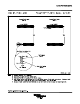
T1: PVDD decoupling capacitors C16, C19, C21, and C24 should be placed very close to PVDD_X pins and ground
return path.
T2: VREG decoupling capacitor C10 should be placed very close to VREG abd AGND pins.
T3: Clear the space above and below the device as much as possible to improve the thermal spreading.
T4: Add many vias to reduce the impedance of ground path through top to bottom side. Make traces as wide as
possible for ground path such as GND_X path.
Figure 15. Printed Circuit Board – Top Layer
Copyright © 2009–2010, Texas Instruments Incorporated Submit Documentation Feedback 21
Product Folder Link(s): DRV8412 DRV8432