
Datasheet


+
-
Inverting
R
IN
R
FB
+
-
C
IN
-IN
Differential
Input
+IN
C
IN
R
IN
R
FB
-IN
R
IN
C
IN
R
FB
Rx
+
-
Cx
Non
Inverting
R
IN
R
FB
C
IN
+IN
DRV603
SLOS617C –JANUARY 2009–REVISED NOVEMBER 2009
www.ti.com
CHARGE PUMP FLYING CAPACITOR AND PVSS CAPACITOR
The charge pump flying capacitor serves to transfer charge during the generation of the negative supply voltage.
The PVSS capacitor must be at least equal to the charge pump capacitor in order to allow maximum charge
transfer. Low-ESR capacitors are an ideal selection, and a value of 1 μF is typical. Capacitor values that are
smaller than 1 μF can be used, but the maximum output voltage may be reduced and the device may not
operate to specifications.
DECOUPLING CAPACITORS
The DRV603 is a DirectPath™ line-driver amplifier that requires adequate power supply decoupling to ensure
that the noise and total harmonic distortion (THD) are low. A good low equivalent-series-resistance (ESR)
ceramic capacitor, typically 1 μF, placed as close as possible to the device V
DD
lead works best. Placing this
decoupling capacitor close to the DRV603 is important for the performance of the amplifier. For filtering
lower-frequency noise signals, a 10-μF or greater capacitor placed near the audio power amplifier would also
help, but it is not required in most applications because of the high PSRR of this device.
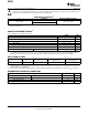
GAIN-SETTING RESISTOR RANGES
The gain-setting resistors, R
IN
and R
fb
, must be chosen so that noise, stability, and input capacitor size of the
DRV603 are kept within acceptable limits. Voltage gain is defined as R
fb
divided by R
IN
.
Selecting values that are too low demands a large input ac-coupling capacitor, C
IN
. Selecting values that are too
high increases the noise of the amplifier. Table 1 lists the recommended resistor values for different gain
settings.
Table 1. Recommended Resistor Values
INPUT RESISTOR FEEDBACK RESISTOR DIFFERENTIAL INPUT NONINVERTING INPUT
INVERTING INPUT GAIN
VALUE, R
IN
VALUE, R
fb
GAIN GAIN
22 kΩ 22 kΩ 1 V/V –1 V/V 2 V/V
15 kΩ 30 kΩ 1.5 V/V –1.5 V/V 2.5 V/V
33 kΩ 68 kΩ 2.1 V/V –2.1 V/V 3.1 V/V
10 kΩ 100 kΩ 10 V/V –10 V/V 11 V/V
Figure 12. Differential, Inverting and Non-Inverting Gain Configurations
10 Submit Documentation Feedback Copyright © 2009, Texas Instruments Incorporated
Product Folder Link(s): DRV603