
Datasheet


Copper
Trace Width
Solder Mask
Thickness
Solder
Pad Width
Solder Mask
Opening
Copper Trace
Thickness
DRV2605
www.ti.com
SLOS825C –DECEMBER 2012–REVISED SEPTEMBER 2014
10 Layout
10.1 Layout Guidelines
Use the following guidelines for the DRV2605 layout:
• The decoupling capacitor for the power supply (V
DD
) should be placed closed to the device pin.
• The filtering capacitor for the regulator (REG) should be placed close to the device REG pin.
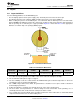
• When creating the pad size for the WCSP pins, TI recommends that the PCB layout use nonsolder mask-
defined (NSMD) land. With this method, the solder mask opening is made larger than the desired land area
and the opening size is defined by the copper pad width. Figure 61 shows and Table 32 lists appropriate
diameters for a wafer-chip scale package (WCSP) layout.
Figure 61. Land Pattern Dimensions
Table 32. Land Pattern Dimensions
SOLDER PAD SOLDER MASK COPPER STENCIL STENCIL
COPPER PAD
DEFINITIONS OPENING THICKNESS OPENING THICKNESS
Nonsolder mask 275 µm 375 µm 275 µm × 275 µm
2
1-oz maximum (32 µm) 125-µm thick
defined (NSMD) (0, –25 µm) (0, –25 µm) (rounded corners)
1. Circuit traces from NSMD defined PWB lands should be 75-µm to 100-µm wide in the exposed area inside
the solder mask opening. Wider trace widths reduce device stand-off and impact reliability.
2. The recommend solder paste is Type 3 or Type 4.
3. The best reliability results are achieved when the PWB laminate glass transition temperature is above the
operating the range of the intended application.
4. For a PWB using a Ni/Au surface finish, the gold thickness should be less 0.5 µm to avoid a reduction in
thermal fatigue performance.
5. Solder mask thickness should be less than 20 µm on top of the copper circuit pattern.
6. The best solder stencil performance is achieved using laser-cut stencils with electro polishing. Use of
chemically-etched stencils results in inferior solder paste volume control.
7. Trace routing away from the WCSP device should be balanced in X and Y directions to avoid unintentional
component movement because of solder-wetting forces.
Copyright © 2012–2014, Texas Instruments Incorporated Submit Documentation Feedback 53
Product Folder Links: DRV2605