
Datasheet


DAC908
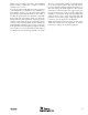
13
SBAS109B
FIGURE 6. Driving a Doubly-Terminated 50Ω Cable Directly.
FIGURE 7. Internal Reference Configuration.
The DC gain for this circuit is equal to feedback resistor R
F
.
At high frequencies, the DAC output impedance (C
D1
, C
D2
)
will produce a zero in the noise gain for the OPA2680 that
may cause peaking in the closed-loop frequency response.
C
F
is added across R
F
to compensate for this noise-gain
peaking. To achieve a flat transimpedance frequency re-
sponse, the pole in each feedback network should be set to:
1
24ππRC
GBP
RC
FF FD
=
(8)
with GBP = Gain Bandwidth Product of OPA
which will give a corner frequency f
-3dB
of approximately:
f
GBP
RC
dB
FD
−
=
3
2π
(9)
The full-scale output voltage is defined by the product of
I
OUTFS
• R
F
, and has a negative unipolar excursion. To
improve on the ac performance of this circuit, adjustment of
R
F
and/or I
OUTFS
should be considered. Further extensions of
this application example may include adding a differential
filter at the OPA2680’s output followed by a transformer, in
order to convert to a single-ended signal.
SINGLE-ENDED CONFIGURATION
Using a single load resistor connected to the one of the DAC
outputs, a simple current-to-voltage conversion can be ac-
complished. The circuit in Figure 6 shows a 50Ω resistor
connected to I
OUT
, providing the termination of the further
connected 50Ω cable. Therefore, with a nominal output
current of 20mA, the DAC produces a total signal swing of
0V to 0.5V into the 25Ω load.
INTERNAL REFERENCE OPERATION
The DAC908 has an on-chip reference circuit that comprises
a 1.24V bandgap reference and a control amplifier. Ground-
ing pin 16, INT/EXT, enables the internal reference opera-
tion. The full-scale output current, I
OUTFS
, of the DAC908 is
determined by the reference voltage, V
REF
, and the value of
resistor R
SET
. I
OUTFS
can be calculated by:
I
OUTFS
= 32 • I
REF
= 32 • V
REF
/ R
SET
(10)
As shown in Figure 7, the external resistor R
SET
connects to
the FSA pin (Full-Scale Adjust). The reference control am-
plifier operates as a V-to-I converter producing a reference
current, I
REF
, which is determined by the ratio of V
REF
and
R
SET
, as shown in Equation 10. The full-scale output current,
I
OUTFS
, results from multiplying I
REF
by a fixed factor of 32.
Different load resistor values may be selected as long as the
output compliance range is not exceeded. Additionally, the
output current, I
OUTFS
, and the load resistor may be mutually
adjusted to provide the desired output signal swing and
performance.
Using the internal reference, a 2kΩ resistor value results in a
20mA full-scale output. Resistors with a tolerance of 1% or
better should be considered. Selecting higher values, the con-
verter output can be adjusted from 20mA down to 2mA.
Operating the DAC908 at lower than 20mA output currents
may be desirable for reasons of reducing the total power
consumption, improving the distortion performance, or observ-
ing the output compliance voltage limitations for a given load
condition.
It is recommended to bypass the REF
IN
pin with a ceramic chip
capacitor of 0.1µF or more. The control amplifier is internally
compensated, and its small signal bandwidth is approximately
1.3MHz. To improve the ac performance, an additional capaci-
tor (C
COMPEXT
) should be applied between the BW pin and the
analog supply, +V
A
, as shown in Figure 7. Using a 0.1µF
capacitor, the small-signal bandwidth and output impedance of
the control amplifier is further diminished, reducing the noise
that is fed into the current source array. This also helps shunting
feedthrough signals more effectively, and improving the noise
performance of the DAC908.
I
OUT
I
OUT
DAC908
25Ω
50Ω
50Ω
I
OUTFS
= 20mA
V
OUT
= 0V to +0.5V
DAC908
C
COMPEXT
0.1µF
C
COMP
400pF
+1.24V Ref.
R
SET
2kΩ
0.1µF
INT/EXT
FSA
BW
+5V
+V
A
REF
IN
Current
Sources
I
REF
=
V
REF
R
SET
Ref
Control
Amp