
Datasheet


DAC8565
SBAS411C –JUNE 2007–REVISED MARCH 2011
www.ti.com
LD1 (DB21) and LD0 (DB20) control the updating of DB21 = 0 and DB20 = 1: Single-channel update.
each analog output with the specified 16-bit data The temporary register and DAC register
value or power-down command. Bit DB19 must corresponding to a DAC selected by DB18 and DB17
always be '0'. The DAC channel select bits (DB18, are updated with the contents of SR data (or
DB17) control the destination of the data (or power-down).
power-down command) from DAC A to DAC D. The
DB21 = 1 and DB20 = 0: Simultaneous update. A
final control bit, PD0 (DB16), selects the power-down
channel selected by DB18 and DB17 updates with
mode of the DAC8565 channels as well as the
the SR data; simultaneously, all the other channels
power-down mode of the internal reference.
update with previously stored data (or power-down)
The DAC8565 supports a number of different load from temporary registers.
commands. The load commands include broadcast
DB21 = 1 and DB20 = 1: Broadcast update. If
commands to address all the DAC8565s on an SPI
DB18 = 0, then SR data are ignored and all channels
bus. The load commands are summarized as follows:
are updated with previously stored data (or
DB21 = 0 and DB20 = 0: Single-channel store. The power-down). If DB18 = 1, then SR data (or
temporary register (data buffer) corresponding to a power-down) updates all channels. Refer to Table 6
DAC selected by DB18 and DB17 updates with the for more information.
contents of SR data (or power-down).
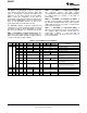
Table 6. Control Matrix for the DAC8565
DB23 DB22 DB21 DB20 DB19 DB18 DB17 DB16 DB15 DB14 DB13-DB0
0 0 LD 1 LD 0 0 DAC Sel 1 DAC Sel 0 PD0 MSB MSB-1 MSB-2...LSB DESCRIPTION
0 0 0 0 0 0 Data Write to buffer A with data
0 0 0 0 1 0 Data Write to buffer B with data
0 0 0 1 0 0 Data Write to buffer C with data
0 0 0 1 1 0 Data Write to buffer D with data
Write to buffer (selected by DB17 and DB18) with
0 0 0 (00, 01, 10, or 11) 1 See Table 7 0
power-down command
Write to buffer with data and load DAC (selected by
0 1 0 (00, 01, 10, or 11) 0 Data
DB17 and DB18)
Write to buffer with power-down command and load
0 1 0 (00, 01, 10, or 11) 1 See Table 7 0
DAC (selected by DB17 and DB18)
Write to buffer with data (selected by DB17 and DB18)
1 0 0 (00, 01, 10, or 11) 0 Data and then load all DACs simultaneously from their
corresponding buffers
Write to buffer with power-down command (selected by
1 0 0 (00, 01, 10, or 11) 1 See Table 7 0 DB17 and DB18) and then load all DACs
simultaneously from their corresponding buffers
Broadcast Modes
0 Simultaneously update all channels of DAC8565 with
X X 1 1 0 X X X
data stored in each channels temporary register
X X 1 1 0 1 X 0 Data Write to all channels and load all DACs with SR data
Write to all channels and load all DACs with
X X 1 1 0 1 X 1 See Table 7 0
power-down command in SR
28 Submit Documentation Feedback Copyright © 2007–2011, Texas Instruments Incorporated
Product Folder Link(s): DAC8565