
Datasheet


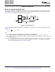


Table Of Contents
- FEATURES
- APPLICATIONS
- DESCRIPTION
- ABSOLUTE MAXIMUM RATINGS
- THERMAL INFORMATION
- ELECTRICAL CHARACTERISTICS
- PIN CONFIGURATIONS
- TIMING REQUIREMENTS
- TABLES OF GRAPHS
- TYPICAL CHARACTERISTICS: Internal Reference
- TYPICAL CHARACTERISTICS: DAC at AVDD = 5.5 V
- TYPICAL CHARACTERISTICS: DAC at AVDD = 3.6 V
- TYPICAL CHARACTERISTICS: DAC at AVDD = 2.7 V
- THEORY OF OPERATION
- APPLICATION INFORMATION
- Revision History

V
REFIN REFOUT
/V
R
R
R
R
V
REF
2
R
DIVIDER
ToOutput Amplifier
DAC8562, DAC8563
DAC8162, DAC8163
DAC7562, DAC7563
www.ti.com
SLAS719D –AUGUST 2010–REVISED AUGUST 2012
Resistor String
The resistor string section is shown in Figure 89. It is simply a string of resistors, each of value R. The code
loaded into the DAC register determines at which node on the string the voltage is tapped off to be fed into the
output amplifier by closing one of the switches connecting the string to the amplifier. The resistor string
architecture guarantees monotonicity. The R
DIVIDER
switch is controlled by the gain registers (see the GAIN
REGISTERS section). Because the output amplifier has a gain of two, R
DIVIDER
is not shorted when the DAC-n
gain is set to one (default if internal reference is disabled), and is shorted when the DAC-n gain is set to two
(default if internal reference is enabled).
Figure 89. Resistor String
Output Amplifier
The output buffer amplifier is capable of generating rail-to-rail voltages on its output, giving a maximum output
range of 0 V to AV
DD
. It is capable of driving a load of 2 kΩ in parallel with 3 nF to GND. The typical slew rate is
0.75 V/µs, with a typical full-scale settling time of 14 µs as shown in Figure 31, Figure 32, Figure 75 and
Figure 76.
Copyright © 2010–2012, Texas Instruments Incorporated Submit Documentation Feedback 27
Product Folder Links: DAC8562 DAC8563 DAC8162 DAC8163 DAC7562 DAC7563