
Datasheet


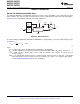


Table Of Contents
- FEATURES
- APPLICATIONS
- DESCRIPTION
- ABSOLUTE MAXIMUM RATINGS
- THERMAL INFORMATION
- ELECTRICAL CHARACTERISTICS
- PIN CONFIGURATIONS
- TIMING REQUIREMENTS
- TABLES OF GRAPHS
- TYPICAL CHARACTERISTICS: Internal Reference
- TYPICAL CHARACTERISTICS: DAC at AVDD = 5.5 V
- TYPICAL CHARACTERISTICS: DAC at AVDD = 3.6 V
- TYPICAL CHARACTERISTICS: DAC at AVDD = 2.7 V
- THEORY OF OPERATION
- APPLICATION INFORMATION
- Revision History

IN
O UT REF
n
D
V = V Gain
2
æ ö
´ ´
ç ÷
è ø
DAC
Gain
Register
Register
REF(+)
Resistor String
REF( )-
GND
V /
V
REFIN
REFOUT
V
OUT
150 kW 150 kW
D
IN
n
DAC8562, DAC8563
DAC8162, DAC8163
DAC7562, DAC7563
SLAS719D –AUGUST 2010–REVISED AUGUST 2012
www.ti.com
THEORY OF OPERATION
DIGITAL-TO-ANALOG CONVERTER (DAC)
The DAC756x, DAC816x, and DAC856x architecture consists of two string DACs, each followed by an output
buffer amplifier. The devices include an internal 2.5-V reference with 4-ppm/°C temperature drift performance.
Figure 88 shows a principal block diagram of the DAC architecture.
Figure 88. DAC Architecture
The input coding to the DAC756x, DAC816x, and DAC856x is straight binary, so the ideal output voltage is given
by Equation 1:
(1)
where:
n = resolution in bits; either 12 (DAC756x), 14 (DAC816x) or 16 (DAC856x)
D
IN
= decimal equivalent of the binary code that is loaded to the DAC register. D
IN
ranges from 0 to 2
n
– 1.
V
REF
= DAC reference voltage; either V
REFOUT
from the internal 2.5-V reference or V
REFIN
from an
aaa external reference.
Gain = 1 by default when internal reference is disabled (using external reference), and gain = 2 by default
aaa when using internal reference. Gain can also be manually set to either 1 or 2 using the gain register.
aaa See the GAIN REGISTERS section for more information.
26 Submit Documentation Feedback Copyright © 2010–2012, Texas Instruments Incorporated
Product Folder Links: DAC8562 DAC8563 DAC8162 DAC8163 DAC7562 DAC7563