
Datasheet


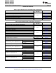
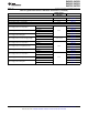

Table Of Contents
- FEATURES
- APPLICATIONS
- DESCRIPTION
- ABSOLUTE MAXIMUM RATINGS
- THERMAL INFORMATION
- ELECTRICAL CHARACTERISTICS
- PIN CONFIGURATIONS
- TIMING REQUIREMENTS
- TABLES OF GRAPHS
- TYPICAL CHARACTERISTICS: Internal Reference
- TYPICAL CHARACTERISTICS: DAC at AVDD = 5.5 V
- TYPICAL CHARACTERISTICS: DAC at AVDD = 3.6 V
- TYPICAL CHARACTERISTICS: DAC at AVDD = 2.7 V
- THEORY OF OPERATION
- APPLICATION INFORMATION
- Revision History

DAC8562, DAC8563
DAC8162, DAC8163
DAC7562, DAC7563
www.ti.com
SLAS719D –AUGUST 2010–REVISED AUGUST 2012
ABSOLUTE MAXIMUM RATINGS
(1)
Over operating free-air temperature range (unless otherwise noted).
VALUE UNIT
AV
DD
to GND –0.3 to 6 V
CLR, D
IN
, LDAC, SCLK and SYNC input voltage to GND –0.3 to AV
DD
+ 0.3 V
V
OUT
to GND –0.3 to AV
DD
+ 0.3 V
V
REFIN
/V
REFOUT
to GND –0.3 to AV
DD
+ 0.3 V
Operating temperature range –40 to 125 °C
Junction temperature, maximum (T
J max
) 150 °C
(1) Stresses beyond those listed under Absolute Maximum Ratings may cause permanent damage to the device. These are stress ratings
only, and functional operation of the device at these or any other conditions beyond those indicated under Recommended Operating
Conditions is not implied. Exposure to absolute-maximum-rated conditions for extended periods may affect device reliability.
THERMAL INFORMATION
DAC856x, DAC816x, DAC756x
THERMAL METRIC DSC DGS UNIT
10 PINS 10 PINS
θ
JA
Junction-to-ambient thermal resistance
(1)
62.8 173.8 °C/W
θ
JCtop
Junction-to-case (top) thermal resistance
(2)
44.3 48.5 °C/W
θ
JB
Junction-to-board thermal resistance
(3)
26.5 79.9 °C/W
ψ
JT
Junction-to-top characterization parameter
(4)
0.4 1.7 °C/W
ψ
JB
Junction-to-board characterization parameter
(5)
25.5 68.4 °C/W
θ
JCbot
Junction-to-case (bottom) thermal resistance
(6)
46.2 N/A °C/W
(1) The junction-to-ambient thermal resistance under natural convection is obtained in a simulation on a JEDEC-standard, high-K board, as
specified in JESD51-7, in an environment described in JESD51-2a.
(2) The junction-to-case (top) thermal resistance is obtained by simulating a cold plate test on the package top. No specific JEDEC-
standard test exists, but a close description can be found in the ANSI SEMI standard G30-88.
(3) The junction-to-board thermal resistance is obtained by simulating in an environment with a ring cold plate fixture to control the PCB
temperature, as described in JESD51-8.
(4) The junction-to-top characterization parameter, ψ
JT
, estimates the junction temperature of a device in a real system and is extracted
from the simulation data for obtaining θ
JA
, using a procedure described in JESD51-2a (sections 6 and 7).
(5) The junction-to-board characterization parameter, ψ
JB
, estimates the junction temperature of a device in a real system and is extracted
from the simulation data for obtaining θ
JA
, using a procedure described in JESD51-2a (sections 6 and 7).
(6) The junction-to-case (bottom) thermal resistance is obtained by simulating a cold plate test on the exposed (power) pad. No specific
JEDEC standard test exists, but a close description can be found in the ANSI SEMI standard G30-88.
Spacer
Copyright © 2010–2012, Texas Instruments Incorporated Submit Documentation Feedback 3
Product Folder Links: DAC8562 DAC8563 DAC8162 DAC8163 DAC7562 DAC7563