
Datasheet


www.ti.com
OPERATION EXAMPLES
DAC8554
SLAS431B – JUNE 2005 – REVISED OCTOBER 2006
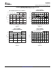
Example 1: Write to Data Buffer A Through Buffer D; Load DAC A Through DAC D Simultaneously
• 1st — Write to data buffer A:
A1 A0 LD1 LD0 DC DAC Sel 1 DAC Sel 0 PD0 DB15 — DB1 DB0
0 0 0 0 X 0 0 0 D15 — D1 D0
• 2nd — Write to data buffer B:
A1 A0 LD1 LD0 DC DAC Sel 1 DAC Sel 0 PD0 DB15 — DB1 DB0
0 0 0 0 X 0 1 0 D15 — D1 D0
• 3rd — Write to data buffer C:
A1 A0 LD1 LD0 DC DAC Sel 1 DAC Sel 0 PD0 DB15 — DB1 DB0
0 0 0 0 X 1 0 0 D15 — D1 D0
• 4th — Write to data buffer D and simultaneously update all DACs:
A1 A0 LD1 LD0 DC DAC Sel 1 DAC Sel 0 PD0 DB15 — DB1 DB0
0 0 1 0 X 1 1 0 D15 — D1 D0
The DAC A, DAC B, DAC C, and DAC D analog outputs simultaneously settle to the specified values upon
completion of the 4th write sequence. (The DAC voltages update simultaneously after the 24th SCLK falling
edge of the 4th write cycle).
Example 2: Load New Data to DAC A Through DAC D Sequentially
• 1st — Write to data buffer A and load DAC A: DAC A output settles to specified value upon completion:
A1 A0 LD1 LD0 DC DAC Sel 1 DAC Sel 0 PD0 DB15 — DB1 DB0
0 0 0 1 X 0 0 0 D15 — D1 D0
• 2nd — Write to data buffer B and load DAC B: DAC B output settles to specified value upon completion:
A1 A0 LD1 LD0 DC DAC Sel 1 DAC Sel 0 PD0 DB15 — DB1 DB0
0 0 0 1 X 0 1 0 D15 — D1 D0
• 3rd — Write to data buffer C and load DAC C: DAC C output settles to specified value upon completion:
A1 A0 LD1 LD0 DC DAC Sel 1 DAC Sel 0 PD0 DB15 — DB1 DB0
0 0 0 1 X 1 0 0 D15 — D1 D0
• 4th — Write to data buffer D and load DAC D: DAC D output settles to specified value upon completion:
A1 A0 LD1 LD0 DC DAC Sel 1 DAC Sel 0 PD0 DB15 — DB1 DB0
0 0 0 1 X 1 1 0 D15 — D1 D0
After completion of each write cycle, DAC analog output settles to the voltage specified.
19
Submit Documentation Feedback