
Datasheet


17
®
DAC7744
ANALOG OUTPUTS
When V
SS
= –15V (dual supply operation), the output ampli-
fier can swing to within 4V of the supply rails, guaranteed
over the –40°C to +85°C temperature range. With V
SS
= 0V
(single-supply operation), and with R
LOAD
also connected to
ground, the output can swing to ground. Care must also be
taken when measuring the zero-scale error when V
SS
= 0V.
Since the output voltage cannot swing below ground, the
output voltage may not change for the first few digital input
codes (0000
H
, 0001
H
, 0002
H
, etc.), if the output amplifier has
a negative offset. At the negative limit of –5mV, the first
specified output starts at code 0021
H
.
Due to the high accuracy of these D/A converters, system
design problems such as grounding and contact resistance
become very important. A 16-bit converter with a 10V full-
scale range has a 1LSB value of 152µV. With a load current
of 1mA, series wiring and connector resistance of only
150mΩ (R
W2
) will cause a voltage drop of 150µV, as shown
in Figure 4. To understand what this means in terms of a
system layout, the resistivity of a typical 1 ounce copper-clad
printed circuit board is 1/2 mΩ per square. For a 1mA load,
a 20 milli-inch wide printed circuit conductor 6 inches long
will result in a voltage drop of 150µV.
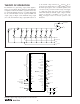
The DAC7744 offers a force and sense output configuration
for the high open-loop gain output amplifiers. This feature
allows the loop around the output amplifier to be closed at
the load, thus ensuring an accurate output voltage, as shown
in Figure 4.
FIGURE 3. Basic Dual-Supply Operation of the DAC7744.
FIGURE 4. Analog Output Closed-Loop Configuration
(1/2 DAC7744). R
W
represents wiring resis-
tances.
DB15 (MSB)
DB14
DB13
DB12
DB11
DB10
DB9
DB8
DB7
DB6
DB5
DB4
DB3
DB2
DB1
DB0 (LSB)
RSTSEL
RST
LOADDACS
R/W
A1
A0
CS
DGND
NC
NC
NC
NC
V
OUT
A Sense
V
OUT
A
V
REF
L AB Sense
V
REF
L AB
V
REF
H AB
V
REF
H AB Sense
V
OUT
B Sense
V
OUT
B
V
OUT
C Sense
V
OUT
C
V
REF
H CD Sense
V
REF
H CD
V
REF
L CD
V
REF
L CD Sense
V
OUT
D Sense
V
OUT
D
V
SS
AGND
V
CC
V
DD
1
2
3
4
5
6
7
8
9
10
11
12
13
14
15
16
17
18
19
20
21
22
23
24
48
47
46
45
44
43
42
41
40
39
38
37
36
35
34
33
32
31
30
29
28
27
26
25
DAC7744
Reset DACs
Data
Bus
Address
Load DAC Registers
READ/WRITE
Chip Select
NC = No Connection
–10V to +10V
–10V
–10V to +10V
–10V to +10V
–10V to +10V
+10V
+10V
–10V
+5V
–15V
0.1µF
1µF
+15V
0.1µF
1µF
+5V
0.1µF
1µF
+
+
+
NC
NC
NC
NC
V
OUT
A Sense
V
OUT
A
V
REF
L AB Sense
V
REF
L AB
V
REF
H AB
V
REF
H AB Sense
V
OUT
B Sense
V
OUT
B
48
47
46
45
44
43
42
41
40
39
38
37
DAC7744
R
W1
R
W2
+10V
+V
V
OUT
R
W1
R
W2
V
OUT
R
LOAD
R
LOAD