
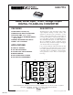
Datasheet


®
2
DAC7715
SPECIFICATIONS (Dual Supply)
At T
A
= –40°C to +85°C, V
CC
= +15V, V
SS
= –15V, V
REFH
= +10V, V
REFL
= –10V, unless otherwise noted.
The information provided herein is believed to be reliable; however, BURR-BROWN assumes no responsibility for inaccuracies or omissions. BURR-BROWN assumes
no responsibility for the use of this information, and all use of such information shall be entirely at the user’s own risk. Prices and specifications are subject to change
without notice. No patent rights or licenses to any of the circuits described herein are implied or granted to any third party. BURR-BROWN does not authorize or warrant
any BURR-BROWN product for use in life support devices and/or systems.
DAC7715U DAC7715UB
PARAMETER CONDITIONS MIN TYP MAX MIN TYP MAX UNITS
ACCURACY
Linearity Error ±2 ±1 LSB
(1)
Linearity Matching
(2)
±2 ±1 LSB
Differential Linearity Error ±1 ±1 LSB
Monotonicity T
MIN
to T
MAX
12 ✻ Bits
Zero-Scale Error Code = 000
H
±2 ✻ LSB
Zero-Scale Drift 1 ✻ ppm/°C
Zero-Scale Matching
(2)
±2 ±1 LSB
Full-Scale Error Code = FFF
H
±2 ✻ LSB
Full-Scale Matching
(2)
±2 ±1 LSB
Power Supply Sensitivity At Full Scale 10 ✻ ppm/V
ANALOG OUTPUT
Voltage Output
(3)
V
REFL
V
REFH
✻✻V
Output Current –5 +5 ✻✻mA
Load Capacitance No Oscillation 500 ✻ pF
Short-Circuit Current ±20 ✻ mA
Short-Circuit Duration To V
SS
, V
CC
, or GND Indefinite ✻
REFERENCE INPUT
V
REFH
Input Range
V
REFL
+1.25
+10 ✻✻V
V
REFL
Input Range –10
V
REFH
– 1.25
✻✻V
Ref High Input Current –0.5 3.0 ✻✻mA
Ref Low Input Current –3.5 0 ✻✻mA
DYNAMIC PERFORMANCE
Settling Time To ±0.012%, 20V Output Step 8 10 ✻✻ µs
Channel-to-Channel Crosstalk
Full-Scale Step
0.25 ✻ LSB
Digital Feedthrough 2 ✻ nV-s
Output Noise Voltage f = 10kHz 65 ✻ nV/√Hz
DIGITAL INPUT
Logic Levels
V
IH
I
IH
≤ ±10µA 3.325 ✻ V
V
IL
I
IL
≤ ±10µA 1.575 ✻ V
Data Format Straight Binary ✻
POWER SUPPLY REQUIREMENTS
V
CC
+14.25 +15.75 ✻✻V
V
SS
–15.75 –14.25 ✻✻V
I
CC
6 8.5 ✻✻ mA
I
SS
–8 –6 ✻✻ mA
Power Dissipation 180 250 ✻✻ mW
TEMPERATURE RANGE
Specified Performance –40 +85 ✻✻°C
NOTES: (1) LSB means Least Significant Bit; if V
REFH
equals +10V and V
REFL
equals –10V, then one LSB equals 4.88mV. (2) All DAC outputs will match within
the specified error band. (3) Ideal output voltage does not take into account zero or full-scale error.