
Datasheet


13
®
DAC7715
ANALOG OUTPUTS
When V
SS
= –15V (dual supply operation), the output
amplifier can swing to within 4V of the supply rails, over
the –40°C to +85°C temperature range. With V
SS
= 0V
(single-supply operation), the output can swing to ground.
Note that the settling time of the output op amp will be
longer with voltages very near ground. Also, care must be
taken when measuring the zero-scale error when V
SS
= 0V.
If the output amplifier has a negative offset, the output
voltage may not change for the first few digital input codes
(000
H
, 001
H
, 002
H
, etc.) since the output voltage cannot
swing below ground.
At the negative offset limit of –4LSB (–9.76mV), for the
single-supply case, the first specified output starts at code
004
H
.
REFERENCE INPUTS
The reference inputs, V
REFL
and V
REFH
, can be any voltage
between V
SS
+ 4V and V
CC
– 4V provided that V
REFH
is at
least 1.25V greater than V
REFL
. The minimum output of
each DAC is equal to V
REFL
– 1LSB plus a small offset
voltage (essentially, the offset of the output op amp). The
maximum output is equal to V
REFH
plus a similar offset
voltage. Note that V
SS
(the negative power supply) must
either be connected to ground or be in the range of –14.75V
to –15.25V. The voltage on V
SS
sets several bias points
within the converter. If V
SS
is not in one of these two
configurations, the bias values may be in error and proper
operation of the device is not guaranteed.
The current into the reference inputs depends on the DAC
output voltages and can vary from a few microamps to
SYMBOL DESCRIPTION MIN TYP MAX UNITS
t
DS
Data Valid to CLK Rising
25 ns
t
DH
Data Held Valid after CLK Rises
20 ns
t
CH
CLK HIGH
30 ns
t
CL
CLK LOW
50 ns
t
CSS
CS LOW to CLK Rising
55 ns
t
CSH
CLK HIGH to CS Rising
15 ns
t
LD1
LOADREG HIGH to CLK Rising
40 ns
t
LD2
CLK Rising to LOADREG LOW
15 ns
t
LDRW
LOADREG LOW Time
45 ns
t
LDDW
LOADDACS LOW Time
45 ns
t
RSSH
RESETSEL Valid to RESET LOW
25 ns
t
RSTW
RESET LOW Time
70 ns
t
S
Settling Time
10 µs
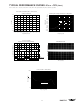
FIGURE 4. DAC7715 Timing.
approximately 3mA. The reference input appears as a vary-
ing load to the reference. If the reference can sink or source
the required current, a reference buffer is not required. See
“Reference Current vs Code” in the Typical Performance
Curves.
The analog supplies must come up before the reference
power supplies, if they are separate. If the power supplies for
the references come up first, then the V
CC
and V
SS
supplies
will be powered from the reference via the ESD protection
diodes (see page 4).
DIGITAL INTERFACE
Figure 4 and Table I provide the basic timing for the
DAC7715. The interface consists of a serial clock (CLK),
serial data (SDI), a load register signal (LOADREG), and a
TABLE I. Timing Specifications (T
A
= –40°C to +85°C).
A1
(MSB) (LSB)
SDI
CLK
CS
LOADREG
A0 X X D11 D10 D9 D3 D2 D1 D0
SDI
CLK
LOADDACS
RESET
V
OUT
t
css
t
LD1
t
CL
t
CH
t
DS
t
DH
t
LD2
t
LDRW
t
LDDW
t
S
t
RSTW
t
RSSH
t
CSH
t
S
1 LSB
ERROR BAND
1 LSB
ERROR BAND
RESETSEL