
Datasheet


0 1 2 3 4 5 6 7 8 9 10
Output Voltage - V
2.445
2.450
2.455
2.460
2.465
2.470
2.475
2.480
2.485
2.490
2.495
2.500
I - mA
SOURCE
AV = 2.7 V,
External Reference = 2.5 V,
DAC Loaded with FFFh
DD
Channel A
0.00
0.10
0.20
0.30
0.40
0.50
0.60
Output Voltage - V
0 1 2 3 4 5 6 7 8 9 10
I - mA
SINK
AV = 2.7 V,
External Reference = 2.5 V,
DAC Loaded with 000h
DD
Channel A
-0.15
-0.10
-0.05
0.00
0.05
0.10
0.15
DAC A DAC B
DAC C DAC D
DAC E DAC F
DAC G DAC H
AV = 2.7 V,
External Reference = 2.5 V
DD
-40 -25 -10 5 20 35 50 65 80 95 110 125
T - Temperature -°C
Gain Error - %FSR
0.00
0.60
0.90
1.50
2.10
2.70
3.00
3.90
4.50
4.70
Power Supply Current - Am
-40 -25 -10 5 20 35 50 65 80 95 110 125
T - Temperature -°C
0.30
1.20
1.80
2.40
3.30
3.60
4.20
AV = 2.7 V,
External Reference = 2.5 V
DD
-0.20
-0.15
-0.10
-0.05
0.00
0.05
0.10
0.15
0.20
DAC A DAC B
DAC C DAC D
DAC E DAC F
DAC G DAC H
AV = 2.7 V,
External Reference = 2.5 V
DD
-40 -25 -10 5 20 35 50 65 80 95 110 125
T - Temperature -°C
Full-Scale Error - %FSR
DAC7678
www.ti.com
SBAS493B –FEBRUARY 2010–REVISED JULY 2012
TYPICAL CHARACTERISTICS: DAC AT AV
DD
= 2.7 V (continued)
At T
A
= 25°C, external reference used, DAC output not loaded, and all DAC codes in straight binary data format, unless
otherwise noted
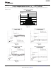
POWER-DOWN CURRENT FULL-SCALE ERROR
vs TEMPERATURE vs TEMPERATURE
Figure 65. Figure 66.
GAIN ERROR
vs TEMPERATURE
Figure 67.
SOURCE CURRENT SINK CURRENT
AT POSITIVE RAIL AT NEGATIVE RAIL
Figure 68. Figure 69.
Copyright © 2010–2012, Texas Instruments Incorporated Submit Documentation Feedback 19
Product Folder Link(s): DAC7678