
Datasheet


8
®
DAC7613
ANALOG OUTPUTS
When V
SS
= –5V (dual supply operation), the output ampli-
fier can swing to within 2.25V of the supply rails, guaran-
teed over the –40°C to +85°C temperature range. With
V
SS
= 0V (single-supply operation), the output can swing to
ground. Note that the settling time of the output op amp will
be longer with voltages very near ground. Additionally, care
must be taken when measuring the zero-scale error when
V
SS
= 0V. Since the output voltage cannot swing below
ground, the output voltage may not change for the first few
digital input codes (000
H
, 001
H
, 002
H
, etc.) if the output
amplifier has a negative offset.
The behavior of the output amplifier can be critical in some
applications. Under short-circuit conditions (DAC output
shorted to ground), the output amplifier can sink a great deal
more current than it can source. See the Specifications table
for more details concerning short-circuit current.
REFERENCE INPUTS
The reference inputs, V
REFL
and V
REFH
, can be any voltage
between V
SS
+ 2.25V and V
DD
– 2.25V provided that V
REFH
is at least 1.25V greater than V
REFL
. The minimum output of
each DAC is equal to V
REFL
plus a small offset voltage
(essentially, the offset of the output op amp). The maximum
output is equal to V
REFH
plus a similar offset voltage. Note
that V
SS
(the negative power supply) must either be
connected to ground or must be in the range of –4.75V to
–5.25V. The voltage on V
SS
sets several bias points within
the converter. If V
SS
is not in one of these two configura-
tions, the bias values may be in error and proper operation
of the device is not guaranteed.
The current into the V
REFH
input depends on the DAC output
voltages and can vary from a few microamps to approxi-
mately 0.1 milliamp. The V
REFH
source will not be required
to sink current, only source it. Bypassing the reference
voltage or voltages with at least a 0.1µF capacitor placed as
close to the DAC7613 package is strongly recommended.
DIGITAL INTERFACE
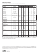
Table I shows the basic control logic for the DAC7613. Note
that the internal register is level triggered and not edge
triggered. When the appropriate signal is LOW, the register
becomes transparent. When this signal is returned HIGH, the
digital word currently in the register is latched. The first
register (the input register) is triggered via the R/W, and CS
inputs. The second register (the DAC register) is transparent
when LOADDAC input is pulled LOW.
The double-buffered architecture is mainly designed so that
the DAC input register can be written at any time and then
the DAC voltage updated by pulling LOADDAC LOW.
INPUT DAC
R/W CS RST LOADDAC REGISTER REGISTER MODE
L L H L Write Write Write
L L H H Write Hold Write Input
H L H H Read Hold Read Input
X H H L Hold Update Update
X H H H Hold Hold Hold
X H L X Hold Reset Reset
X = Don’t Care.
TABLE I. DAC7613 Control Logic Truth Table.