
Datasheet


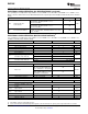

ELECTRICAL CHARACTERISTICS (DC SPECIFICATIONS)
(1)
DAC5686
www.ti.com
............................................................................................................................................................ SLWS147F – APRIL 2003 – REVISED JUNE 2009
over operating free-air temperature range, AVDD = 3.3 V, CLKVDD = 3.3 V, PLLVDD = 3.3 V, IOVDD = 3.3 V,
DVDD = 1.8 V, IOUT
FS
= 20 mA (unless otherwise noted)
PARAMETER TEST CONDITIONS MIN TYP MAX UNIT
Resolution 16
DC Accuracy
(2)
INL Integral nonlinearity 1 LSB = IOUT
FS
/2
16
, T
MIN
to T
MAX
12 LSB
1.84e – 4 IOUT
FS
DNL Differential nonlinearity 9 LSB
1.37e – 4 IOUT
FS
Analog Output
Coarse gain linearity (INL) LSB = 1/10
th
of full scale 0.016 LSB
Fine gain linearity (INL) 3 LSB
Offset error Mid-code offset 0.003 %FSR
Without internal reference 0.7
Gain error %FSR
With internal reference 0.7
Gain mismatch With internal reference, dual DAC, – 2 2 %FSR
SSB mode
Full-scale output current
(3)
2 20 mA
Output compliance range
(4)
IOUT
FS
= 20 mA AVDD – 0.5 AVDD + 0.5 V
Output resistance 300 k Ω
Output capacitance 5 pF
Reference Output
Reference voltage 1.14 1.2 1.26 V
Reference output current
(5)
100 nA
Reference Input
V
EXTIO
Input voltage range 0.1 1.25 V
Input resistance 1 M Ω
Small-signal bandwidth 2.5 kHz
Input capacitance 100 pF
Temperature Coefficients
ppm of
Offset drift 3
FSR/C
Without internal reference 15
ppm of
Gain drift
FSR/C
With internal reference 40
Reference voltage drift 25 ppm/C
(1) Specifications subject to change without notice.
(2) Measured differential across IOUTA1 and IOUTA2 or IOUTB1 and IOUTB2 with 25 Ω each to AVDD
(3) Nominal full-scale current, IOUT
FS
, equals 16 × the IBIAS current.
(4) The upper limit of the output compliance is determined by the CMOS process. Exceeding this limit may result in transistor breakdown,
resulting in reduced reliability of the DAC5686 device. The lower limit of the output compliance is determined by the load resistors and
full-scale output current. Exceeding the upper limit adversely affects distortion performance and integral nonlinearity.
(5) Use an external buffer amplifier with high-impedance input to drive any external load.
Copyright © 2003 – 2009, Texas Instruments Incorporated Submit Documentation Feedback 7
Product Folder Link(s): DAC5686