
Datasheet


DAC5686
SLWS147F – APRIL 2003 – REVISED JUNE 2009 ............................................................................................................................................................
www.ti.com
Unmatched gains and offsets at the RF quadrature modulator result in unwanted sideband and local oscillator
feedthrough. Each DAC in the DAC5686 has an 11-bit offset adjustment and 12-bit gain adjustment, which
compensate for quadrature modulator input imbalances, thus reducing RF filtering requirements.
In quadrature modulation mode, on-chip mixing provides baseband-to-IF up-conversion. Mixing frequencies are
flexibly chosen with a 32-bit programmable NCO. Channel carrier selection is performed at baseband by complex
mixing in the ASIC/FPGA. Baseband I and Q from the ASIC/FPGA are input to the DAC5686, which interpolates
the low data-rate signal to higher data rates. The single DAC output from the DAC5686 is the final IF
single-sideband spectrum presented to RF.
The 2 × , 4 × , 8 × , and 16 × interpolation filters are implemented as a cascade of half-band 2 × interpolation filters.
Unused filters for interpolation rates of less than 16 × are shut off to reduce power consumption. The DAC5686
provides a full bypass mode, which enables the user to bypass all the interpolation and mixing.
The DAC5686 PLL clock multiplier controls all internal clocks for the digital filters and the DAC cores. The
differential clock input and internal clock circuitry provides for optimum jitter performance. Sine wave clock input
signal is supported. The PLL can be bypassed by an external clock running at the DAC core update rate. The
clock divider of the PLL ensures that the digital filters operate at the correct clock frequencies.
The DAC5686 operates with an analog supply voltage of 3.3 V and a digital supply voltage of 1.8 V. Digital I/Os
are 1.8-V and 3.3-V CMOS compatible. Power dissipation is 950 mW at maximum operating conditions. The
DAC5686 provides a nominal full-scale differential current output of 20 mA, supporting both single-ended and
differential applications. The output current can be directly fed to the load with no additional external output buffer
required. The device has been specifically designed for a differential transformer-coupled output with a 50- Ω
doubly terminated load. For a 20-mA full-scale output current, both a 4:1 impedance ratio (resulting in an output
power of 4 dBm) and 1:1 impedance ratio transformer ( – 2-dBm output power) are supported.
The DAC5686 operational modes are configured by programming registers through a serial interface. The serial
interface can be configured to either a 3- or 4-pin interface allowing it to communicate with many
industry-standard microprocessors and microcontrollers. Data (I and Q) can be input to the DAC5686 as
separate parallel streams on two data buses, or as a single interleaved data stream on one data bus.
An accurate on-chip 1.2-V temperature-compensated band-gap reference and control amplifier allows the user to
adjust the full-scale output current from 20 mA down to 2 mA. This provides 20-dB gain range control
capabilities. Alternatively, an external reference voltage can be applied for maximum flexibility. The device
features a SLEEP mode, which reduces the standby power to approximately 10 mW, thereby minimizing the
system power consumption.
The DAC5686 is available in a 100-pin HTQFP package. The device is characterized for operation over the
industrial temperature range of – 40C to 85C.
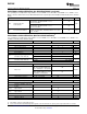
ORDERING INFORMATION
T
A
PACKAGE DEVICES
100 HTQFP
(1)
(PZP) PowerPAD™ plastic quad flatpack
– 40C to 85C
DAC5686IPZP
(1) Thermal pad size: 6 mm × 6 mm
2 Submit Documentation Feedback Copyright © 2003 – 2009, Texas Instruments Incorporated
Product Folder Link(s): DAC5686