
Datasheet


DAC3484
www.ti.com
SLAS749C –MARCH 2011–REVISED AUGUST 2012
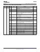
Register name: config5 – Address: 0x05, Default: Setup and Power-Up Conditions Dependent (WRITE TO
CLEAR)
Register Address Default
Bit Name Function
Name Value
config5 0x05 15 alarm_from_zerochk This alarm indicates the 8-bit FIFO write pointer address has an all NA
zeros patterns. Due to pointer address being a shift register, this is
not a valid address and will cause the write pointer to be stuck until
the next sync. This error is typically caused by timing error or
improper power start-up sequence. If this alarm is asserted,
resynchronization of FIFO is necessary. See Power-Up Sequence
for more detail.
14 Reserved Reserved for factory use. NA
13:11 alarms_from_fifo(2:0) Alarm indicating FIFO pointer collisions and nearness: NA
MM 000: All fine
MM 001: Pointers are 2 away
MM 01x: Pointers are 1 away
MM 1xx: FIFO pointer collision
If the FIFO pointer collision alarm is set when collisiongone_ena is
enabled, the FIFO must be re-synchronized and the bits must be
cleared to resume normal operation.
10 alarm_dacclk_gone Alarm indicating the DACCLK has been stopped. If the bit is set NA
when dacclkgone_ena is enabled, the DACCLK must resume and
the bit must be cleared to resume normal operation.
9 alarm_dataclk_gone Alarm indicating the DATACLK has been stopped. If the bit is set NA
when dataclkgone_ena is enabled, the DATACLK must resume and
the bit must be cleared to resume normal operation.
8 alarm_output_gone Alarm indicating either alarm_dacclk_gone, alarm_dataclk_gone, or NA
alarm_fifo_collision are asserted. It controls the output. When high it
will output "0x8000" for each output connected to the DAC. If the bit
is set when dacclkgone_ena, dataclkgone_ena, or
collisiongone_ena are enabled, then the corresponding errors must
be fixed and the bits must be cleared to resume normal operation.
7 alarm_from_iotest Alarm indicating the input data pattern does not match the pattern in NA
the iotest_pattern registers. When data pattern checker mode is
enabled, this alarm in register config5, bit7 is the only valid alarm.
Other alarms in register config5 are not valid and can be
disregarded.
6 Reserved Reserved for factory use. NA
5 alarm_from_pll Alarm indicating the PLL has lost lock. For version ID "100" or NA
earlier, alarm_from_PLL may not indicate the correct status of the
PLL. Refer to pll_lfvolt(2:0) in register config24 for proper PLL lock
indication.
4 alarm_rparity Alarm indicating a parity error on data captured on the rising edge NA
of DATACLKP/N.
3 alarm_fparity Alarm indicating a parity error on data captured on the falling edge NA
of DATACLKP/N.
2 alarm_frame_parity Alarm indicating a parity error when using the FRAME as parity bit. NA
1 Reserved Reserved for factory use. NA
0 Reserved Reserved for factory use. NA
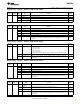
Register name: config6 – Address: 0x06, Default: No RESET Value (READ ONLY)
Register Default
Address Bit Name Function
Name Value
config6 0x06 15:8 tempdata(7:0) This is the output from the chip temperature sensor. The value of this register in No
two’s complement format represents the temperature in degrees Celsius. This RESET
register must be read with a minimum SCLK period of 1μs. Value
7:2 Reserved Reserved for factory use. 000000
1 Reserved Reserved for factory use. 0
0 Reserved Reserved for factory use. 0
Copyright © 2011–2012, Texas Instruments Incorporated Submit Documentation Feedback 35
Product Folder Links: DAC3484