
Datasheet


I
OUT
DAC2904
R
L
26.1W
R
L
28.7W
R
4
402W
R
3
200W
R
2
402W
R
1
200W
OPA690
C
OPT
+5V
V
OUT
-5V
I
OUT
DAC2904
-V =I R
OUT OUT F1
·
R
F1
R
F2
C
F1
C
F2
C
D1
C
D2
I
OUT
50W
50W
-5V
+5V
I
OUT
I
OUT
-V
OUT
=
R
F2
·
1/2
OPA2690
1/2
OPA2690
DAC2904
SBAS198C –AUGUST 2001–REVISED OCTOBER 2009..............................................................................................................................................
www.ti.com
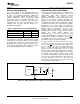
DIFFERENTIAL CONFIGURATION USING AN slew-limitations or into an overload condition; both
OP AMP would cause excessive distortion. The difference
amplifier can easily be modified to add a level shift for
If the application requires a dc-coupled output, a
applications requiring the single-ended output voltage
difference amplifier may be considered, as shown in
to be unipolar; that is, swing between 0V and +2V.
Figure 21. Four external resistors are needed to
configure the voltage-feedback op amp OPA690 as a
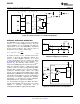
DUAL TRANSIMPEDANCE OUTPUT
difference amplifier performing the differential to
CONFIGURATION
single-ended conversion. Under the configuration
shown, the DAC2904 generates a differential output
The circuit example of Figure 22 shows the signal
signal of 0.5V
PP
at the load resistors, R
L
. The resistor
output currents connected into the summing junctions
values shown were selected to result in a symmetric
of the dual voltage-feedback op amp OPA2690 that is
25Ω loading for each of the current outputs since the
set up as a transimpedance stage, or -to-V converter.
input impedance of the difference amplifier is in
With this circuit, the DAC output will be kept at a
parallel to resistors R
L
, and should be considered.
virtual ground, minimizing the effects of output
impedance variations, which results in the best dc
linearity (INL). As mentioned previously, care should
be taken not to drive the amplifier into slew-rate
limitations, and produce unwanted distortion.
Figure 21. Difference Amplifier Provides
Differential to Single-Ended Conversion and
DC-Coupling
The OPA690 is configured for a gain of two.
Therefore, operating the DAC2904 with a 20mA
full-scale output will produce a voltage output of ±1V.
This requires the amplifier to operate off of a dual
power supply (±5V). The tolerance of the resistors
typically sets the limit for the achievable
common-mode rejection. An improvement can be
obtained by fine-tuning resistor R
4
.
This configuration typically delivers a lower level of ac
Figure 22. Dual, Voltage-Feedback Amplifier
OPA2690 Forms Differential Transimpedance
performance than the previously discussed
Amplifier
transformer solution because the amplifier introduces
another source of distortion. Suitable amplifiers
should be selected based on the slew rate, harmonic
The dc gain for this circuit is equal to feedback
distortion, and output swing capabilities. High-speed
resistor R
F
. At high frequencies, the DAC output
amplifiers like the OPA690 or OPA687 may be
impedance (C
D1
, C
D2
) will produce a zero in the noise
considered. The ac performance of this circuit may be
gain for the OPA2690 that may cause peaking in the
improved by adding a small capacitor, C
DIFF
, between
closed-loop frequency response.
the outputs I
OUT
and I
OUT
(see Figure 21). This will
introduce a real pole to create a low-pass filter in
order to slew-limit the DAC fast output signal steps,
which otherwise could drive the amplifier into
14 Submit Documentation Feedback Copyright © 2001–2009, Texas Instruments Incorporated
Product Folder Link(s): DAC2904