
Datasheet


SCLK
DAC128S085
SYNC
V
OUTA
V
OUTB
V
OUTC
V
OUTD
V
REF1
D
IN
D
OUT
V
REF2
V
OUTE
V
OUTF
V
OUTG
V
OUTH
Set offset and gain
Programmable I
SOURCE
Set Limits for Range Detector
+V
- V
+
-
+
-
V
IN
Bipolar Output Swing
Control (Valve, Damper, Robotics,
Process Ctrl) or Voltage Setpoint
(Battery Ctrl, Signal Trigger)
Setting Sensor Drive or Supply
(Add buffer for sensor with low
input impedance)
V
REF
ADC121S625
Set ADC Reference
Sensor
Signal
(Ch A - Ch D)
(Ch E - Ch H)
3V or 5V Reference
3V or 5V Reference
Output to Another
DAC (Daisy Chain)
DAC128S085
SNAS407F –AUGUST 2007–REVISED MARCH 2013
www.ti.com
APPLICATION CIRCUITS
The following figures are examples of the DAC128S085 in typical application circuits. These circuits are basic
and will generally require modification for specific circumstances.
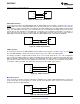
Industrial Application
Figure 38 shows the DAC128S085 controlling several different circuits in an industrial setting. Channel A is
shown providing the reference voltage to the ADC121S625, one of Texas Instruments' general purpose Analog-
to-Digital Converters (ADCs). The reference for the ADC121S625 may be set to any voltage from 0.2V to 5.5V,
providing the widest dynamic range possible. Typically, the ADC121S625 will be monitoring a sensor and would
benefit from the ADC's reference voltage being adjustable. Channel B is providing the drive or supply voltage for
a sensor. By having the sensor supply voltage adjustable, the output of the sensor can be optimized to the input
level of the ADC monitoring it. Channel C is defined to adjust the offset or gain of an amplifier stage in the
system. Channel D is configured with an opamp to provide an adjustable current source. Being able to convert
one of the eight channels of the DAC128S085 to a current output eliminates the need for a separate current
output DAC to be added to the circuit. Channel E, in conjunction with an opamp, provides a bipolar output swing
for devices requiring control voltages that are centered around ground. Channel F and G are used to set the
upper and lower limits for a range detector. Channel H is reserved for providing voltage control or acting as a
voltage setpoint.
Figure 38. Industrial Application
ADC Reference
Figure 39 shows Channel A of the DAC128S085 providing the drive or supply voltage for a bridge sensor. By
having the sensor supply voltage adjustable, the output of the sensor can be optimized to the input level of the
ADC monitoring it. The output of the sensor is amplified by a fixed gain amplifier stage with a differential gain of 1
+ 2 × (R
F
/ R
I
). The advantage of this amplifier configuration is the high input impedance seen by the output of
the bridge sensor. The disadvantage is the poor common-mode rejection ratio (CMRR). The common-mode
voltage (V
CM
) of the bridge sensor is half of Channel A's DAC output. The V
CM
is amplified by a gain of 1V/V by
the amplifier stage and thus becomes the bias voltage for the input of the ADC121S705. Channel B of the
DAC128S085 is providing the reference voltage to the ADC121S705. The reference for the ADC121S705 may
be set to any voltage from 1V to 5V, providing the widest dynamic range possible.
The reference voltage for Channel A and B is powered by an external 5V power supply. Since the 5V supply is
common to the sensor supply voltage and the reference voltage of the ADC, fluctuations in the value of the 5V
supply will have a minimal effect on the digital output code of the ADC. This type of configuration is often referred
to as a "Ratio-metric" design. For example, an increase of 5% to the 5V supply will cause the sensor supply
voltage to increase by 5%. This causes the gain or sensitivity of the sensor to increase by 5%. The gain of the
amplifier stage is unaffected by the change in supply voltage. The ADC121S705 on the other hand, also
24 Submit Documentation Feedback Copyright © 2007–2013, Texas Instruments Incorporated
Product Folder Links: DAC128S085