
Datasheet


SCLK
SYNC
t
SS
1
17
t
SH
1615
DAC128S085
www.ti.com
SNAS407F –AUGUST 2007–REVISED MARCH 2013
OUTPUT AMPLIFIERS
The output amplifiers are rail-to-rail, providing an output voltage range of 0V to V
A
when the reference is V
A
. All
amplifiers, even rail-to-rail types, exhibit a loss of linearity as the output approaches the supply rails (0V and V
A
,
in this case). For this reason, linearity is specified over less than the full output range of the DAC. However, if the
reference is less than V
A
, there is only a loss in linearity in the lowest codes.
The output amplifiers are capable of driving a load of 2 kΩ in parallel with 1500 pF to ground or to V
A
. The zero-
code and full-scale outputs for given load currents are available in the Electrical Characteristics.
REFERENCE VOLTAGE
The DAC128S085 uses dual external references, V
REF1
and V
REF2
, that are shared by channels A, B, C, D and
channels E, F, G, H respectively. The reference pins are not buffered and have an input impedance of 30 kΩ. It
is recommended that V
REF1
and V
REF2
be driven by voltage sources with low output impedance. The reference
voltage range is 0.5V to V
A
, providing the widest possible output dynamic range.
SERIAL INTERFACE
The three-wire interface is compatible with SPI™, QSPI and MICROWIRE, as well as most DSPs and operates
at clock rates up to 40 MHz. A valid serial frame contains 16 falling edges of SCLK. See Figure 1 for information
on a write sequence.
A write sequence begins by bringing the SYNC line low. Once SYNC is low, the data on the D
IN
line is clocked
into the 16-bit serial input register on the falling edges of SCLK. To avoid mis-clocking data into the shift register,
it is critical that SYNC not be brought low on a falling edge of SCLK (see minimum and maximum setup times for
SYNC in A.C. and Timing Characteristics and Figure 29). On the 16th falling edge of SCLK, the last data bit is
clocked into the register. The write sequence is concluded by bringing the SYNC line high. Once SYNC is high,
the programmed function (a change in the DAC channel address, mode of operation and/or register contents) is
executed. To avoid mis-clocking data into the shift register, it is critical that SYNC be brought high between the
16th and 17th falling edges of SCLK (see minimum and maximum hold times for SYNC in A.C. and Timing
Characteristics and Figure 29).
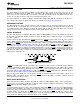
Figure 29. CS Setup and Hold Times
If SYNC is brought high before the 15th falling edge of SCLK, the write sequence is aborted and the data that
has been shifted into the input register is discarded. If SYNC is held low beyond the 17th falling edge of SCLK,
the serial data presented at D
IN
will begin to be output on D
OUT
. More information on this mode of operation can
be found in DAISY CHAIN OPERATION. In either case, SYNC must be brought high for the minimum specified
time before the next write sequence is initiated with a falling edge of SYNC.
Since the D
IN
buffer draws more current when it is high, it should be idled low between write sequences to
minimize power consumption. On the other hand, SYNC should be idled high to avoid the activation of daisy
chain operation where D
OUT
is active.
DAISY CHAIN OPERATION
Daisy chain operation allows communication with any number of DAC128S085s using a single serial interface.
As long as the correct number of data bits are input in a write sequence (multiple of sixteen bits), a rising edge of
SYNC will properly update all DACs in the system.
To support multiple devices in a daisy chain configuration, SCLK and SYNC are shared across all DAC128S085s
and D
OUT
of the first DAC in the chain is connected to D
IN
of the second. Figure 30 shows three DAC128S085s
connected in daisy chain fashion. Similar to a single channel write sequence, the conversion for a daisy chain
operation begins on a falling edge of SYNC and ends on a rising edge of SYNC. A valid write sequence for n
devices in a chain requires n times 16 falling edges to shift the entire input data stream through the chain. Daisy
chain operation is guaranteed for a maximum SCLK speed of 30MHz.
Copyright © 2007–2013, Texas Instruments Incorporated Submit Documentation Feedback 15
Product Folder Links: DAC128S085