
Datasheet


DAC1280
1
2
3
4
5
6
7
8 9
10
11
12
13
14
15
16
CLK
TDATA
SYNC
DGND
DVDD
GAIN0
GAIN1
GAIN2
VREF
RREF
AVSS
AVDD
NC
IOUTN
IOUTP
PWDN
DAC1280
SBAS432A –APRIL 2010–REVISED SEPTEMBER 2010
www.ti.com
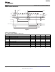
DEVICE INFORMATION
PW PACKAGE
TSSOP-16
(TOP VIEW)
TERMINAL FUNCTIONS
TERMINAL
NAME NO. I/O DESCRIPTION
CLK 1 Digital Input 4.096MHz master clock
TDATA 2 Digital Input Bitstream digital data
SYNC 3 Digital Input Synchronize control
DGND 4 Digital Ground Digital ground
DVDD 5 Digital Supply Digital power supply
GAIN0 6 Digital Input Gain select 0
GAIN1 7 Digital Input Gain select 1
GAIN2 8 Digital Input Gain select 2
VREF 9 Analog Input Voltage reference input
RREF 10 Analog Full-scale range resistor
AVSS 11 Analog Supply Negative analog power supply, V
REF
common, R
REF
common
AVDD 12 Analog Supply Positive analog power supply
NC 13 — No connection; do not connect externally.
IOUTN 14 Analog Output Negative signal output current
IOUTP 15 Analog Output Positive signal output current
PWDN 16 Digital Input Power-down control; active low
6 Submit Documentation Feedback Copyright © 2010, Texas Instruments Incorporated
Product Folder Link(s): DAC1280