
Datasheet


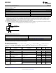


Table Of Contents

I/O
GND
TO INTERNAL
CIRCUITRY
DAC104S085
SNAS362F –MAY 2006–REVISED MARCH 2013
www.ti.com
Operating Ratings
(1)(2)
Operating Temperature Range −40°C ≤ T
A
≤ +125°C
Supply Voltage, V
A
+2.7V to 5.5V
Reference Voltage, V
REFIN
+1.0V to V
A
Digital Input Voltage
(3)
0.0V to 5.5V
Output Load 0 to 1500 pF
SCLK Frequency Up to 40 MHz
(1) Absolute Maximum Ratings indicate limits beyond which damage to the device may occur. Operating Ratings indicate conditions for
which the device is functional, but do not ensure specific performance limits. For ensured specifications and test conditions, see the
Electrical Characteristics. The ensured specifications apply only for the test conditions listed. Some performance characteristics may
degrade when the device is not operated under the listed test conditions. Operation of the device beyond the maximum Operating
Ratings is not recommended.
(2) All voltages are measured with respect to GND = 0V, unless otherwise specified.
(3) The inputs are protected as shown below. Input voltage magnitudes up to 5.5V, regardless of V
A
, will not cause errors in the conversion
result. For example, if V
A
is 3V, the digital input pins can be driven with a 5V logic device.
Package Thermal Resistances
(1)
Package θ
JA
10-Lead VSSOP 240°C/W
10-Lead SON 250°C/W
Soldering process must comply with Reflow Temperature Profile specifications. Refer to http://www.ti.com/lit/SNOA549.
(1) Reflow temperature profiles are different for lead-free packages.
Electrical Characteristics
The following specifications apply for V
A
= +2.7V to +5.5V, V
REFIN
= V
A
, C
L
= 200 pF to GND, f
SCLK
= 30 MHz, input code
range 12 to 1011. Boldface limits apply for T
MIN
≤ T
A
≤ T
MAX
and all other limits are at T
A
= 25°C, unless otherwise
specified.
Units
Symbol Parameter Conditions Typical
(1)
Limits
(1)
(Limits)
STATIC PERFORMANCE
Resolution 10 Bits (min)
Monotonicity 10 Bits (min)
INL Integral Non-Linearity ±0.7 ±2 LSB (max)
+0.08 +0.35 LSB (max)
DNL Differential Non-Linearity V
A
= 2.7V to 5.5V
−0.03 −0.25 LSB (min)
ZE Zero Code Error I
OUT
= 0 +5 +15 mV (max)
FSE Full-Scale Error I
OUT
= 0 −0.1 −0.75 %FSR (max)
GE Gain Error All ones Loaded to DAC register −0.2 −1.0 %FSR
ZCED Zero Code Error Drift −20 µV/°C
V
A
= 3V −0.7 ppm/°C
TC GE Gain Error Tempco
V
A
= 5V −1.0 ppm/°C
(1) Typical figures are at T
J
= 25°C, and represent most likely parametric norms. Test limits are specified to TI's AOQL (Average Outgoing
Quality Level).
4 Submit Documentation Feedback Copyright © 2006–2013, Texas Instruments Incorporated
Product Folder Links: DAC104S085