
Datasheet


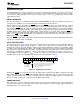


Table Of Contents

V
A
R
R
R
R
To Output Amplifier
R
DAC104S085
SNAS362F –MAY 2006–REVISED MARCH 2013
www.ti.com
FUNCTIONAL DESCRIPTION
DAC SECTION
The DAC104S085 is fabricated on a CMOS process with an architecture that consists of switches and resistor
strings that are followed by an output buffer. The reference voltage is externally applied at V
REFIN
and is shared
by all four DACs.
For simplicity, a single resistor string is shown in Figure 29. This string consists of 1024 equal valued resistors
with a switch at each junction of two resistors, plus a switch to ground. The code loaded into the DAC register
determines which switch is closed, connecting the proper node to the amplifier. The input coding is straight
binary with an ideal output voltage of:
V
OUTA,B,C,D
= V
REFIN
x (D / 1024) (2)
where D is the decimal equivalent of the binary code that is loaded into the DAC register. D can take on any
value between 0 and 1023. This configuration ensures that the DAC is monotonic.
Figure 29. DAC Resistor String
OUTPUT AMPLIFIERS
The output amplifiers are rail-to-rail, providing an output voltage range of 0V to V
A
when the reference is V
A
. All
amplifiers, even rail-to-rail types, exhibit a loss of linearity as the output approaches the supply rails (0V and V
A
,
in this case). For this reason, linearity is specified over less than the full output range of the DAC. However, if the
reference is less than V
A
, there is only a loss in linearity in the lowest codes. The output capabilities of the
amplifier are described in the Electrical Tables.
The output amplifiers are capable of driving a load of 2 kΩ in parallel with 1500 pF to ground or to V
A
. The zero-
code and full-scale outputs for given load currents are available in the Electrical Characteristics Table.
14 Submit Documentation Feedback Copyright © 2006–2013, Texas Instruments Incorporated
Product Folder Links: DAC104S085