
Datasheet


DAC081S101
SNAS323C –JUNE 2005–REVISED FEBRUARY 2013
www.ti.com
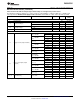
Electrical Characteristics
Values shown in this table are design targets and are subject to change before product release.
The following specifications apply for V
A
= +2.7V to +5.5V, R
L
= 2kΩ to GND, C
L
= 200 pF to GND, f
SCLK
= 30 MHz, input
code range 4 to 251. Boldface limits apply for T
MIN
≤ T
A
≤ T
MAX
: all other limits T
A
= 25°C, unless otherwise specified.
Units
Parameter Test Conditions Typical
(1)
Limits
(1)
(Limits)
STATIC PERFORMANCE
Resolution 8 Bits (min)
Monotonicity 8 Bits (min)
INL Integral Non-Linearity +0.16 +0.75 LSB (max)
−0.12 −0.75 LSB (min)
+0.04 +0.1 LSB (max)
DNL Differential Non-Linearity
−0.02 −0.1 LSB (min)
ZE Zero Code Error I
OUT
= 0 +3.8 +15 mV (max)
FSE Full-Scale Error I
OUT
= 0 −0.07 −1.0 %FSR (max)
GE Gain Error All ones Loaded to DAC register −0.10 ±1.0 %FSR (max)
ZCED Zero Code Error Drift −20 µV/°C
V
A
= 3V −0.7 ppm/°C
TC GE Gain Error Tempco
V
A
= 5V −1.0 ppm/°C
OUTPUT CHARACTERISTICS
0 V (min)
Output Voltage Range
(2)
V
A
V (max)
V
A
= 3V, I
OUT
= 10 µA 2.0 mV
V
A
= 3V, I
OUT
= 100 µA 5.0 mV
ZCO Zero Code Output
V
A
= 5V, I
OUT
= 10 µA 3.0 mV
V
A
= 5V, I
OUT
= 100 µA 5.4 mV
V
A
= 3V, I
OUT
= 10 µA 2.986 V
V
A
= 3V, I
OUT
= 100 µA 2.976 V
FSO Full Scale Output
V
A
= 5V, I
OUT
= 10 µA 4.976 V
V
A
= 5V, I
OUT
= 100 µA 4.970 V
R
L
= ∞ 1500 pF
Maximum Load Capacitance
R
L
= 2kΩ 1500 pF
DC Output Impedance 1.3 Ohm
V
A
= 5V, V
OUT
= 0V,
−63 mA
Input code = FFh
V
A
= 3V, V
OUT
= 0V,
−50 mA
Input code = FFh
I
OS
Output Short Circuit Current
V
A
= 5V, V
OUT
= 5V,
74 mA
Input code = 00h
V
A
= 3V, V
OUT
= 3V,
53 mA
Input code = 00h
(1) Typical figures are at T
J
= 25°C, and represent most likely parametric norms. Test limits are guaranteed to TI's AOQL (Average
Outgoing Quality Level).
(2) This parameter is guaranteed by design and/or characterization and is not tested in production.
4 Submit Documentation Feedback Copyright © 2005–2013, Texas Instruments Incorporated
Product Folder Links: DAC081S101