
Datasheet


I/O
GND
TO INTERNAL
CIRCUITRY
DAC081S101
www.ti.com
SNAS323C –JUNE 2005–REVISED FEBRUARY 2013
Absolute Maximum Ratings
(1)(2)
Supply Voltage, V
A
6.5V
Voltage on any Input Pin −0.3V to (V
A
+ 0.3V)
Input Current at Any Pin
(3)
10 mA
Package Input Current
(3)
20 mA
Power Consumption at T
A
= 25°C See
(4)
ESD Susceptibility
(5)
Human Body Model 2500V
Machine Model 250V
Soldering Temperature, Infrared,
10 Seconds
(6)
235°C
Storage Temperature −65°C to +150°C
(1) Absolute Maximum Ratings indicate limits beyond which damage to the device may occur. Operating Ratings indicate conditions for
which the device is functional, but do not guarantee specific performance limits. For guaranteed specifications and test conditions, see
the Electrical Characteristics. The guaranteed specifications apply only for the test conditions listed. Some performance characteristics
may degrade when the device is not operated under the listed test conditions.
(2) All voltages are measured with respect to GND = 0V, unless otherwise specified
(3) When the input voltage at any pin exceeds the power supplies (that is, less than GND, or greater than V
A
), the current at that pin should
be limited to 10 mA. The 20 mA maximum package input current rating limits the number of pins that can safely exceed the power
supplies with an input current of 10 mA to two.
(4) The absolute maximum junction temperature (T
J
max) for this device is 150°C. The maximum allowable power dissipation is dictated by
T
J
max, the junction-to-ambient thermal resistance (θ
JA
), and the ambient temperature (T
A
), and can be calculated using the formula
P
D
MAX = (T
J
max − T
A
) / θ
JA
. The values for maximum power dissipation will be reached only when the device is operated in a severe
fault condition (e.g., when input or output pins are driven beyond the power supply voltages, or the power supply polarity is reversed).
Obviously, such conditions should always be avoided.
(5) Human body model is 100 pF capacitor discharged through a 1.5 kΩ resistor. Machine model is 220 pF discharged through ZERO
Ohms.
(6) See the section entitled "Surface Mount" found in any post 1986 National Semiconductor Linear Data Book for methods of soldering
surface mount devices.
Operating Ratings
(1)(2)
Operating Temperature Range −40°C ≤ T
A
≤ +105°C
Supply Voltage, V
A
(3)
+2.7V to 5.5V
Any Input Voltage
(4)
−0.1 V to (V
A
+ 0.1 V)
Output Load 0 to 1500 pF
SCLK Frequency Up to 30 MHz
(1) Absolute Maximum Ratings indicate limits beyond which damage to the device may occur. Operating Ratings indicate conditions for
which the device is functional, but do not guarantee specific performance limits. For guaranteed specifications and test conditions, see
the Electrical Characteristics. The guaranteed specifications apply only for the test conditions listed. Some performance characteristics
may degrade when the device is not operated under the listed test conditions.
(2) All voltages are measured with respect to GND = 0V, unless otherwise specified
(3) To guarantee accuracy, it is required that V
A
be well bypassed.
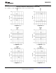
(4) The analog inputs are protected as shown below. Input voltage magnitudes up to V
A
+ 300 mV or to 300 mV below GND will not
damage this device. However, errors in the conversion result can occur if any input goes above V
A
or below GND by more than 100 mV.
For example, if V
A
is 2.7V
DC
, ensure that −100mV ≤ input voltages ≤2.8V
DC
to ensure accurate conversions.
Package Thermal Resistances
Package θ
JA
8-Lead VSSOP 240°C/W
6-Lead SOT 250°C/W
Copyright © 2005–2013, Texas Instruments Incorporated Submit Documentation Feedback 3
Product Folder Links: DAC081S101