
Datasheet


CY74FCT16374T
CY74FCT162374T
2
Maximum Ratings
[2, 3]
(Above which the useful life may be impaired. For user
guidelines, not tested.)
Storage Temperature .............................. −55°C to +125°C
Ambient Temperature with
Power Applied.......................................... −55°C to +125°C
DC Input Voltage................................................. −0.5V to +7.0V
DC Output Voltage.............................................. −0.5V to +7.0V
DC Output Current
(Maximum Sink Current/Pin)............................−60 to +120 mA
Power Dissipation ..........................................................1.0W
Static Discharge Voltage............................................>2001V
(per MIL-STD-883, Method 3015)
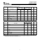
Function Table
[1]
Inputs Outputs
FunctionD CLK OE O
X L H Z High-Z
X H H Z
L L L Load
Register
H L H
L H Z
H H Z
Pin Description
Name Description
D Data Inputs
CLK Clock Inputs
OE Three-State Output Enable Inputs (Active LOW)
O Three-State Outputs
Operating Range
Range
Ambient
Temperature V
CC
Industrial −40°C to +85°C 5V ± 10%
Electrical Characteristics Over the Operating Range
Parameter Description Test Conditions Min. Typ.
[4]
Max. Unit
V
IH
Input HIGH Voltage 2.0 V
V
IL
Input LOW Voltage 0.8 V
V
H
Input Hysteresis
[5]
100 mV
V
IK
Input Clamp Diode Voltage V
CC
=Min., I
IN
=−18 mA −0.7 −1.2 V
I
IH
Input HIGH Current V
CC
=Max., V
I
=V
CC
±1 µA
I
IL
Input LOW Current V
CC
=Max., V
I
=GND ±1 µA
I
OZH
High Impedance Output Current
(Three-State Output pins)
V
CC
=Max., V
OUT
=2.7V ±1 µA
I
OZL
High Impedance Output Current
(Three-State Output pins)
V
CC
=Max., V
OUT
=0.5V ±1 µA
I
OS
Short Circuit Current
[6]
V
CC
=Max., V
OUT
=GND −80 −140 −200 mA
I
O
Output Drive Current
[6]
V
CC
=Max., V
OUT
=2.5V −50 −180 mA
I
OFF
Power-Off Disable V
CC
=0V, V
OUT
≤4.5V
[7]
±1 µA
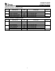
Output Drive Characteristics for CY74FCT16374T
Parameter Description Test Conditions Min. Typ.
[4]
Max. Unit
V
OH
Output HIGH Voltage V
CC
=Min., I
OH
=−3 mA 2.5 3.5 V
V
CC
=Min., I
OH
=−15 mA 2.4 3.5 V
V
CC
=Min., I
OH
=−32 mA 2.0 3.0 V
V
OL
Output LOW Voltage V
CC
=Min., I
OL
=64 mA 0.2 0.55 V
Notes:
1. H = HIGH Voltage Level. L = LOW Voltage Level. X = Don’t Care. Z = HIGH Impedance. = LOW-to-HIGH Transition.
2. Operation beyond the limits set forth may impair the useful life of the device. Unless otherwise noted, these limits are over the operating free-air temperature
range.
3. Unused inputs must always be connected to an appropriate logic voltage level, preferably either V
CC
or ground.
4. Typical values are at V
CC
= 5.0V, T
A
= +25˚C ambient.
5. This parameter is specified but not tested.
6. Not more than one output should be shorted at a time. Duration of short should not exceed one second. The use of high-speed test apparatus and/or sample
and hold techniques are preferable in order to minimize internal chip heating and more accurately reflect operational values. Otherwise prolonged shorting
of a high output may raise the chip temperature well above normal and thereby cause invalid readings in other parametric tests. In any sequence of parameter
tests, I
OS
tests should be performed last.
7. Tested at +25˚C.