
Datasheet


CLC006
8
4
3
1
5
2
V
CC
6
7
R1
154:
R4
75:
V
EE
R3
154:
R5
75:
J1
-
+
U1
CLC006
8
4
3
1
5
2
V
CC
6
7
J2
V
IN-
R1
154:
R4
75:
V
EE
R3
154:
R5
75:
J1
V
IN+
-
+
U1
CLC006
8
4
3
1
5
2
V
CC
6
7
-
+
V
TT
V
EE
Z
0
Z
0
ECL Output
= Z
0
= Z
0
CLC006
www.ti.com
SNLS015G –AUGUST 1998–REVISED APRIL 2013
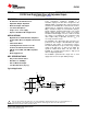
Figure 5. DC Coupled Input
Figure 6. Single Ended 50Ω ECL input Figure 7. Differential 50Ω ECL Input
OUTPUT INTERFACING
The CLC006’s class AB output stage, Figure 8, requires no standing current in the output transistors and
therefore requires no biasing or pull-down resistors. Advantages of this arrangement are lower power dissipation
and fewer external components. The output may be either D.C. or A.C. coupled to the load. A bandgap voltage
reference sets output voltage levels which are compatible with F100K and 10K ECL when correctly terminated.
The outputs do not have the same output voltage temperature coefficient as 10K. Therefore, noise margins will
be reduced over the full temperature range when driving 10K ECL. Noise margins will not be affected when
interfacing to F100K since F100K is fully voltage and temperature compensated.
Copyright © 1998–2013, Texas Instruments Incorporated Submit Documentation Feedback 5
Product Folder Links: CLC006