
Datasheet


CD/74HC4051, CD54/74HCT4051, CD54/74HC4052,
www.ti.com
SCHS122J –NOVEMBER 1997–REVISED FEBRUARY 2011
Absolute Maximum Ratings
(1) (2)
over operating free-air temperature range (unless otherwise noted)
MIN MAX UNIT
V
CC
– V
EE
DC supply voltage –0.5 10.5 V
V
CC
DC supply voltage –0.5 7 V
V
EE
DC supply voltage 0.5 –7 V
I
IK
DC input diode current V
I
< – 0.5 V or V
I
> V
CC
+ 0.5 V ±20 mA
I
OK
DC switch diode current V
I
< V
EE
– 0.5 V or V
I
> V
CC
+ 0.5 V ±20 mA
DC switch current V
I
> V
EE
– 0.5 V or V
I
< V
CC
+ 0.5 V ±25 mA
I
CC
DC V
CC
or ground current ±50 mA
I
EE
DC V
EE
current –20 mA
E (PDIP) package 67
M (SOIC) package 73
θ
JA
Package thermal impedance
(3)
°C/W
NS (SOP) package 64
PW (TSSOP) package 108
Maximum junction temperature 150 °C
Maximum storage temperature range –65 150 °C
Maximum lead temperature (soldering 10 s) 300 °C
(1) Stresses beyond those listed under "absolute maximum ratings" may cause permanent damage to the device. These are stress ratings
only, and functional operation of the device at these or any other conditions beyond those indicated under "recommended operating
conditions" is not implied. Exposure to absolute-maximum-rated conditions for extended periods may affect device reliability.
(2) All voltages referenced to GND unless otherwise specified.
(3) The package thermal impedance is calculated in accordance with JESD 51-7.
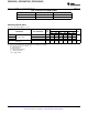
Recommended Operating Conditions
For maximum reliability, nominal operating conditions should be selected so that operation is always within the following
ranges.
PARAMETER MIN MAX UNIT
CD54/74HC types 2 6
Supply voltage range
V
CC
(1)
V
(T
A
= full package temperature range)
CD54/74HCT types 4.5 5.5
Supply voltage range CD54/74HC types, CD54/74HCT types
V
CC
– V
EE
2 10 V
(T
A
= full package temperature range) (see Figure 1)
Supply voltage range CD54/74HC types, CD54/74HCT types
V
EE
(2)
0 –6 V
(T
A
= full package temperature range) (see Figure 2)
V
I
DC input control voltage GND V
CC
V
V
IS
Analog switch I/O voltage V
EE
V
CC
V
T
A
Operating temperature –55 125 °C
2 V 0 1000
t
r
, t
f
Input rise and fall times 4.5 V 0 500 ns
6 V 0 400
(1) All voltages referenced to GND unless otherwise specified.
(2) In certain applications, the external load resistor current may include both V
CC
and signal line components. To avoid drawing V
CC
current when switch current flows into the transmission gate inputs, the voltage drop across the bidirectional switch must not exceed
0.6 V (calculated from r
ON
values shown in Electrical Specifications table). No V
CC
current will flow through R
L
if the switch current flows
into terminal 3 on the HC/HCT4051; terminals 3 and 13 on the HC/HCT4052; terminals 4, 14, and 15 on the HC/HCT4053.
© 1997–2011, Texas Instruments Incorporated Submit Documentation Feedback 7
Product Folder Link(s): CD/74HC4051, CD54/74HCT4051, CD54/74HC4052,