
Datasheet


bq76PL536A-Q1
SLUSAM3 –MAY 2011
www.ti.com
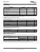
ABSOLUTE MAXIMUM RATINGS
over operating free-air temperature range (unless otherwise noted)
(1)
VALUE UNIT
Supply voltage range, V
MAX
BAT1, BAT2
(2)
–0.3 to 36 V
VC1–VC6 –0.3 to 36
VC0 –0.3 to 2
VCn to VCn-1, n=1 to 6 0 to 36
TS1+, TS1–, TS2+, TS2– –0.3 to 6
Input voltage range, V
IN
V
GPAI –0.3 to 6
GPIO –0.3 to V
REG50
+ 0.3
DRDY_N, SDO_N, FAULT_N, ALERT_N V
BAT
– 1 to V
BAT
+ 2
CONV_S, SDI_S, SCLK_S, CS_S –2 to 1
CONV_N, SDI_N, SCLK_N, CS_N –0.3 to 36
DRDY_S, SDO_S, FAULT_S, ALERT_S –0.3 to 5
Output voltage range, V
O
GPIO –0.3 to V
REG50
+ 0.3 V
CB1…CB6 (CBREF = 0x00) –0.3 to 36
REG50, AUX –0.3 to 6
Junction temperature 150 °C
Storage temperature range, T
stg
–65 to 150 °C
(1) Stresses beyond those listed under Absolute Maximum Ratings may cause permanent damage to the device. These are stress ratings
only; functional operation of the device at these or any other conditions beyond those indicated under Recommended Operating
Conditions is not implied. Exposure to absolute-maximum-rated conditions for extended periods may affect device reliability.
(2) All voltages are with respect to VSS of this device except where otherwise noted.
RECOMMENDED OPERATING CONDITIONS
Typical values stated where T
A
= 25ºC and V
BAT
= 20 V, Min/Max values stated where T
A
= –40˚C to 105ºC and V
BAT
= 7.2 V
to 30 V (unless otherwise noted)
MIN NOM MAX UNIT
V
BAT
Supply voltage BAT 7.2 27 V
VCn–VC(n – 1)
(1)
1 4.5
GPAI 0 2.5
GPIO 0 V
REG50
CBn
(1)
VC(n – 1) VCn
V
I
, Input
voltage TS1+, TS1–, TS2+, TS2– 0 V
REG50
/2 V
range
Non-top IC in stack DRDY_N, SDO_N, FAULT_N, ALERT_N BAT + 1
Top IC in stack DRDY_N, SDO_N, FAULT_N, ALERT_N BAT
Non-bottom IC in stack CONV_S, SDI_S, SCLK_S, CS_S –1
Bottom IC in stack CONV_S, SDI_S, SCLK_S, CS_S VSS
Non-bottom IC in stack CONV_N, SDI_N, SCLK_N, CS_N 1
V
O
,
Bottom IC in stack CONV_N, SDI_N, SCLK_N, CS_N VSS
Output
V
voltage
Non-top IC in stack DRDY_S, SDO_S, FAULT_S, ALERT_S BAT – 1
range
Top IC in stack DRDY_S, SDO_S, FAULT_S, ALERT_S BAT
C
REG50
External capacitor REG50 pin 2.2 µF
C
VREF
External capacitor V
REF
pin 9.2 10 15 µF
C
LDO
External capacitor LDOx pin 2.2 3.3 µF
T
OPR
Operating temperature
(2)
–40 105 °C
(1) n = 1 to 6
(2) Device specifications stated within this range.
6 Submit Documentation Feedback Copyright © 2011, Texas Instruments Incorporated
Product Folder Link(s): bq76PL536A-Q1