
Datasheet


bq76PL536A-Q1
www.ti.com
SLUSAM3 –MAY 2011
Table 2. Fault Detection Summary (continued)
SIGNALING
FAULT DETECTION PIN
DEVICE_STATUS
X_STATUS BIT SET
BIT SET
HSEL = 1 HSEL = 0
CRC
(1)
CRC fail on received packet FAULT_S FAULT_H FAULT FAULT_STATUS[CRC]
CUV V
Cx
< V
UV
for t
UV
FAULT_S FAULT_H FAULT FAULT_STATUS[CUV]
COV V
Cx
> V
OV
for t
OV
FAULT_S FAULT_H FAULT FAULT_STATUS[COV]
AR Address ≠ (0x01→ 0x3e) ALERT_S ALERT_H ALERT ALERT_STATUS[AR]
Protected-register Parity not even in protected
ALERT_S ALERT_H ALERT ALERT_STATUS[PARITY]
parity error register
EPROM single-bit ECC logic fault detected and
ALERT_S ALERT_H ALERT ALERT_STATUS[ECC_COR]
error corrected
FORCE User set FORCE bit ALERT_S ALERT_H ALERT ALERT_STATUS[FORCE]
Die temperature ≥
Thermal shutdown ALERT_S ALERT_H ALERT ALERT_STATUS[TSD]
TSD
THRESHOLD
SLEEP IC exited SLEEP mode ALERT_S ALERT_H ALERT ALERT_STATUS[SLEEP]
OT2 V
TS2
> V
OT
for t
OT
ALERT_S ALERT_H ALERT ALERT_STATUS[OT2]
OT1 V
TS1
> V
OT
for t
OT
ALERT_S ALERT_H ALERT ALERT_STATUS[OT1]
(1) The CRC fault may be prevented from setting the FAULT pin by setting IO_CONFIG[7] = 1. The FAULT_STATUS[CRC] bit is still set
when CRC error is detected, but the FAULT pin remains de-asserted.
Fault Recovery Procedure
When any error flag in DEVICE_STATUS[], FAULT_STATUS[], or ALERT_STATUS[] is set and latched, the
state can only be cleared by host communication via SPI. Writing to the respective FAULT_STATUS or
ALERT_STATUS register bit with a 1 clears the latch for that bit. The exceptions are the two FORCE bits, which
are cleared by writing a 0 to the bit.
The FAULT_STATUS[] and ALERT_STATUS[] register bits are read-only, with the exception of the FORCE bit,
which may be directly written to either a 1 or 0.
Secondary Protector Built-In Self-Test Features
The secondary protector functions have built-in test for verifying the connections through the signal chain of ICs
in the stack back to the host CPU. This verifies the wiring, connections, and signal path through the ICs by
forcing a current through the signal path.
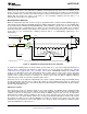
To implement this feature, host firmware should set the FAULT[FORCE] or ALERT[FORCE] bit in the top-most
device in the stack. The device asserts the associated pin on the South interface, and it propagates down the
stack, back to the base device. The base device in turn asserts the FAULT_H (ALERT_H) pin to the host,
allowing the host to check for the received signal and thereby verify correct operation.
CELL BALANCING
The bq76PL536A-Q1 has six dedicated outputs (CB1…CB6) that can be used to control external N-FETs as part
of a cell balancing system. The implementation of appropriate algorithms is controlled by the system host. The
CB_CTRL[CBAL1–6] bits control the state of each of the outputs. The outputs are copied from the bit state of the
CB_CTRL register, i.e., a 1 in this register activates the external balance FET by placing a high on the
associated pin.
The CBx pins switch between approximately the positive and negative voltages of the cell across which the
external FET is connected. This allows the use of a small, low-cost N-FET in series with a power resistor to
provide cell balancing,.
Cell Balance Control Safety Timer
The CBx outputs are cleared when the internal safety timer expires. The internal safety timer (CB_TIME) value is
programmed in units of seconds or minutes (range set by CB_CTRL bit 7) with an accuracy of ±10%.
The timer begins when any CB_CTRL bit changes from 0 to 1. The timer is reset if all CB_CTRL bits are
Copyright © 2011, Texas Instruments Incorporated Submit Documentation Feedback 23
Product Folder Link(s): bq76PL536A-Q1