
Datasheet


High
Frequency
Current
Path
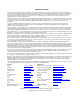
L1 R1
C3
C1
C2
PGND
SW
V
OUT
Super
Capacitor
V
IN
Charge Current Direction
To SRP and SRN pin
R
SNS
To Inductor To Capacitor and Output
Current Sensing Direction
bq24640
www.ti.com
SLUSA44 –MARCH 2010
Figure 14. High Frequency Current Path
Figure 15. Sensing Resistor PCB Layout
Refer to the EVM design (SLUU410) for the recommended component placement with trace and via locations.
For the QFN information, refer to SCBA017 and SLUA271A.
Copyright © 2010, Texas Instruments Incorporated Submit Documentation Feedback 21
Product Folder Link(s): bq24640