
Datasheet


bq24616
www.ti.com
SLUSA49B –APRIL 2010– REVISED OCTOBER 2011
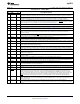
Pin Functions – 24-Pin QFN
PIN
FUNCTION DESCRIPTION
NO. NAME I/O
1 ACN I Adapter current-sense resistor, negative input. A 0.1-μF ceramic capacitor is placed from ACN to ACP to provide
differential-mode filtering. An optional 0.1-μF ceramic capacitor is placed from the ACN pin to GND for common-mode filtering.
2 ACP I Adapter current-sense resistor, positive input. A 0.1-μF ceramic capacitor is placed from ACN to ACP to provide
differential-mode filtering. A 0.1-μF ceramic capacitor is placed from the ACP pin to GND for common-mode filtering.
3 ACDRV O AC adapter to system MOSFET driver output. Connect through a 1-kΩ resistor to the gate of the ACFET P-channel power
MOSFET and the reverse-conduction-blocking P-channel power MOSFET. The internal gate drive is asymmetrical, allowing a
quick turnoff and slow turnon, in addition to the internal break-before-make logic with respect to BATDRV. If needed, an optional
capacitor from gate to source of the ACFET is used to slow down the ON and OFF times.
4 CE I Charge-enable active-HIGH logic input. HI enables charge. LO disables charge. It has an internal 1-MΩ pulldown resistor.
5 STAT1 O Open-drain charge-status pin to indicate various charger operations (See Table 3)
6 TS I Temperature qualification voltage input for battery-pack negative-temperature-coefficient thermistor. Program the hot and cold
temperature window with a resistor divider from VREF to TS to GND. (See Figure 17)
7 TTC I Fast-charge safety timer and termination control. Connect a capacitor from this node to GND to set the timer. When this input is
LOW, the fast-charge timer and termination are disabled. When this input is HIGH, the fast-charge timer is disabled, but
termination is allowed.
8 PG O Open-drain power-good status output. Active-LOW when IC has a valid VCC (not in UVLO or ACOV or SLEEP mode).
Active-HIGH when IC has an invalid VCC. PG can be used to drive an LED or communicate with a host processor.
9 STAT2 O Open-drain charge-status pin to indicate various charger operations (See Table 3)
10 VREF O 3.3-V regulated voltage output. Place a 1-μF ceramic capacitor from VREF to GND pin close to the IC. This voltage could be
used for programming of voltage and current regulation and for programming the TS threshold.
11 ISET1 I Fast-charge current-set input. The voltage on the ISET1 pin programs the fast-charge current-regulation set-point. To avoid early
termination during the V
T1
and V
T2
range, fast-charge current must be higher than 2 times the termination current.
12 VFB I Output-voltage analog-feedback adjustment. Connect the output of a resistive voltage divider from the battery terminals to this
node to adjust the output battery-regulation voltage.
13 SRN I/O Charge current-sense resistor, negative input. A 0.1-μF ceramic capacitor is placed from SRN to SRP to provide
differential-mode filtering. An optional 0.1-μF ceramic capacitor is placed from the SRN pin to GND for common-mode filtering.
14 SRP I/O Charge current-sense resistor, positive input. A 0.1-μF ceramic capacitor is placed from SRN to SRP to provide differential-mode
filtering. A 0.1-μF ceramic capacitor is placed from the SRP pin to GND for common-mode filtering.
15 ISET2 I Pre-charge and termination current-set input. The voltage of ISET2 pin programs the pre-charge current-regulation set-point and
termination-current trigger point.
16 ACSET I Adapter current-set input. The voltage on the ACSET pin programs the input current-regulation set-point during dynamic power
management (DPM)
17 GND Low-current sensitive analog/digital ground. On PCB layout, connect with thermal underneath the IC.
18 REGN O PWM low-side driver positive 6-V supply output. Connect a 1-μF ceramic capacitor from REGN to the GND pin, close to the IC.
Use for low-side driver and high-side driver bootstrap voltage by connecting a small-signal Schottky diode from REGN to BTST.
19 LODRV O PWM low-side driver output. Connect to the gate of the low-side power MOSFET with a short trace.
20 PH I PWM high-side driver negative supply. Connect to the phase-switching node (junction of the low-side power MOSFET drain,
high-side power MOSFET source, and output inductor).
21 HIDRV O PWM high-side driver output. Connect to the gate of the high-side power MOSFET with a short trace.
22 BTST I PWM high-side driver positive supply. Connect the 0.1-μF bootstrap capacitor from PH to BTST, and a bootstrap Schottky diode
from REGN to BTST.
23 BATDRV O Battery to system MOSFET driver output. Gate drive for the battery to system load BAT PMOS power FET to isolate the system
from the battery to prevent current flow from the system to the battery, while allowing a low-impedance path from battery to
system. Connect this pin through a 1-kΩ resistor to the gate of the input BAT P-channel MOSFET. Connect the source of the
FET to the system load-voltage node. Connect the drain of the FET to the battery-pack positive terminal. The internal gate drive
is asymmetrical to allow a quick turnoff and slow turnon, in addition to the internal break-before-make logic with respect to
ACDRV. If needed, an optional capacitor from gate to source of the BATFET is used to slow down the ON and OFF times.
24 VCC I IC power positive supply. Connect through a 10-Ω resistor to the common-source (diode-OR) point: source of high-side
P-channel MOSFET and source of reverse-blocking power P-channel MOSFET. Place a 1-μF ceramic capacitor from VCC to
GND pin close to the IC.
Thermal pad Exposed pad beneath the IC. Always solder the thermal pad to the board, and have vias on the thermal pad plane
star-connecting to GND and to the ground plane for a high-current power converter. It also serves as a thermal pad to dissipate
the heat.
Copyright © 2010–2011, Texas Instruments Incorporated Submit Documentation Feedback 13
Product Folder Link(s): bq24616