
Datasheet


www.ti.com
ABSOLUTE MAXIMUM RATINGS
(1)
DISSIPATION RATINGS
RECOMMENDED OPERATING CONDITIONS
ELECTRICAL CHARACTERISTICS
VOLTAGE REGULATION
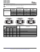
bq24200, bq24201
bq24202, bq24203
bq24204, bq24205
SLUS501C – OCTOBER 2001 – REVISED MARCH 2008
over operating free-air temperature range (unless otherwise noted)
VALUE UNIT
Supply voltage (Vcc with respect to GND) 16.5 V
Input voltage, IN, STAT, TS (all with respect to GND) 16.5 V
Input voltage, BAT, OUT (all with respect to GND) 7 V
Output sink/source current (STAT) 15 mA
T
stg
Storage temperature range – 65 to 150 ° C
T
J
Junction temperature range – 40 to 125 ° C
Lead temperature (soldering, 10 sec) 300 ° C
(1) Stresses beyond those listed under absolute maximum ratings may cause permanent damage to the device. These are stress ratings
only, and functional operation of the device at these or any other conditions beyond those indicated under recommended operating
conditions is not implied. Exposure to absolute maximum rated conditions for extended periods may affect device reliability.
THERMAL IMPEDANCE THERMAL IMPEDANCE T
A
≤ 25 ° C DERATING FACTOR
PACKAGE
JUNCTION-TO-AMBIENT ( θ
JA
) JUNCTION-TO-CASE ( θ
JC
) POWER RATING ABOVE T
A
= 25 ° C
8 Pin DGN
(1)
57.20 ° C/W 4.4 ° C/W 1.75 W 0.017 W/ ° C
(1) This data is based on using JEDEC High-K board and topside traces, top and bottom thermal pad (2 mm × 3 mm), internal 1 oz. power
and ground planes, four thermal via underneath the die connecting to ground plane.
MIN MAX UNIT
V
CC
Supply voltage V
(LOWV-MIN)
13.5
V
V
IN
Input voltage V
(LOWV-MIN)
13.5
T
J
Operating junction temperature range – 40 125 ° C
over 0 ° C ≤ T
J
≤ 125 ° C and supply voltage range (unless otherwise noted)
PARAMETER TEST CONDITIONS MIN TYP MAX UNIT
I
CC(VCC)
Vcc Current Vcc > Vcc(min) 1.7 2.5 mA
Sum of currents into OUT and BAT pins, Vcc < 5 µ A
V
(SLP)
, 0 ° C ≤ T
J
≤ 85 ° C
I
CC(SLP)
Sleep current
Sum of currents into OUT and BAT pins, Vcc < 10 µ A
V
(SLP)
I
CC(STDBY
Standby current Sum of currents into Vcc, IN and TS pins, 1 mA
)
(Vcc – V
I(TS)
) ≤ 300 mV
I
IB(BAT)
Input bias current on BAT pin 1 µ A
I
IB(TB)
Input bias current on TS pin 0.1 × Vcc ≤ V
I(TS)
≤ 0.8 × Vcc 1 µ A
V
O(REG)
+ V
(DO.MAX)
≤ VCC, I
(TERM)
< I
O(OUT)
≤ 500 mA, over 0 ° C ≤ T
J
≤ 125 ° C and supply voltage range (unless otherwise noted)
PARAMETER TEST CONDITIONS MIN TYP MAX UNIT
V
O(REG)
+ V
(DO – MAX)
≤ 10 V, I
(TERM)
< I
O(OUT)
≤ 250 mA 4.0795 4.10 4.1205 V
4.05 4.10 4.15 V
V
O(REG)
Output voltage
V
O(REG)
+ V
(DO – MAX)
≤ 10 V, I
(TERM)
< I
O(OUT)
≤ 250 mA 4.1790 4.20 4.2210 V
4.15 4.20 4.25 V
V
(DO)
Dropout voltage (V
(IN)
– V
(OUT)
) V
O(REG)
+ V
(DO – MAX)
≤ Vcc, I
O(OUT)
= 500 mA 200 350 500 mV
Copyright © 2001 – 2008, Texas Instruments Incorporated Submit Documentation Feedback 3
Product Folder Link(s): bq24200, bq24201 bq24202, bq24203 bq24204, bq24205