
Datasheet


bq24030, bq24031
bq24032A, bq24035, bq24038
www.ti.com
............................................................................................................................................... SLUS618H –AUGUST 2004–REVISED OCTOBER 2009
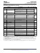
ELECTRICAL CHARACTERISTICS (continued)
over junction temperature range (0°C ≤ T
J
≤ 125°C) and the recommended supply voltage range (unless otherwise noted)
PARAMETER TEST CONDITIONS MIN TYP MAX UNIT
STAT1, STAT2. ACPG AND USBPG, PG OPEN DRAIN (OD) OUTPUTS
(15)
I
OL
= 5 mA, An external pullup
V
OL
Low-level output saturation voltage 0.25 V
resistor ≥ 1 K required.
I
LKG
Input leakage current 1 5 μA
ISET2, CE, VBSEL INPUTS
V
IL
Low-level input voltage 0 0.4
V
V
IH
High-level input voltage 1.4
I
IL
Low-level input current, CE –1
I
IH
High-level input current, CE 1
I
IL
Low-level input current, ISET2 V
ISET2
= 0 V –20
μA
I
IH
High-level input current, ISET2 V
ISET2
= V
CC
40
I
IL1
Low-level input current VBSEL = Low 6 1
I
IH1
High-level input current VBSEL = High 15
t
(CE-HLDOFF)
Holdoff time, CE CE going low only 3.3 6.2 ms
PSEL INPUT
V
IL
Low-level input voltage Falling Hi→Low; 280 K ± 10% applied when low. 0.975 1 1.025 V
V
IL
+
V
IH
High-level input voltage Input R
PSEL
sets external hysteresis V
IL
+ 0.01 V
0.024
I
IL
Low-level input current, PSEL –1 μA
I
IH
High-level input current, PSEL μA
TIMERS
K
(TMR)
Timer set factor t
(CHG)
= K
(TMR)
× R
(TMR)
0.313 0.360 0.414 s/Ω
R
(TMR)
(16)
External resistor limits 30 100 kΩ
0.09 × 0.10 × 0.11 ×
t
(PRECHG)
Precharge timer s
t
(CHG)
t
(CHG)
t
(CHG)
Timer fault recovery pullup from
I
(FAULT)
1 kΩ
OUT to BAT
CHARGER SLEEP THRESHOLDS (ACPG , PG, and USBPG THRESHOLDS, LOW → POWER GOOD)
V
VCC
≤
V
(SLPENT)
V
(UVLO)
≤ V
I(BAT)
≤ V
O(BAT-REG)
,
Sleep-mode entry threshold V
I(BAT)
(17)
No t
(BOOT-UP)
delay
+125 mV
V
V
VCC
≥
V
(SLPEXIT)
V
(UVLO)
≤ V
I(BAT)
≤ V
O(BAT-REG)
,
Sleep-mode exit threshold V
I(BAT)
(17)
No t
(BOOT-UP)
delay
+190 mV
R
(TMR)
= 50 kΩ,
t
(DEGL)
Deglitch time for sleep mode
(18)
V
(AC)
or V
(USB)
or decreasing below threshold, 100-ns fall 22.5 ms
time, 10-mv overdrive
(15) See Charger Sleep mode for ACPG (V
CC
= V
AC
) and USBPG (V
CC
= V
USB
) specifications.
(16) To disable the fast-charge safety timer and charge termination, tie TMR to the LDO pin. Tying the TMR pin high changes the timing
resistor from the external value to an internal 50 kΩ ±25%, which can add an additional tolerance to any timed spectification. The TMR
pin normally regulates to 2.5 V when the charge current is not restricted by the DPPM or thermal feedback loops. If these loops become
active, the TMR pin voltage will be reduced proportionally to the reduction in charge current and the clock frequency will be reduced by
the same percentage (timed durations will count down slower, extending their time). The TMR pin is clamped at 0.80 V, for a maximum
time extension of 2.5 V ÷ 0.8 V × 100 = 310%.
(17) The IC is considered in sleep mode when both AC and USB are absent (ACPG = USBPG = OPEN DRAIN).
(18) Does not declare sleep mode until after the deglitch time and implement the needed power transfer immediately according to the
switching specification.
Copyright © 2004–2009, Texas Instruments Incorporated Submit Documentation Feedback 7
Product Folder Link(s): bq24030, bq24031 bq24032A, bq24035, bq24038