
Datasheet


AM3517, AM3505
www.ti.com
SPRS550E –OCTOBER 2009–REVISED MARCH 2013
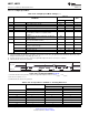
Table 6-133. Y Parameter
CLKD Y
1 or Even 0.5
Odd (trunc[CLKD/2])/CLKD
6.7.1.2 MMC/SD/SDIO in High-Speed MMC Mode
The following tables assume testing over the recommended operating conditions and electrical
characteristic conditions.
Table 6-134. MMC/SD/SDIO Timing Conditions High-Speed MMC Mode
TIMING CONDITION PARAMETER 1.8V, 3.3V UNIT
MIN MAX
High-Speed MMC Mode
Input Conditions
t
r
Input signal rise time 0.19 3 ns
t
f
Input signal fall time 0.19 3 ns
Output Conditions
C
LOAD
Output load capacitance 30 pF
Table 6-135. MMC/SD/SDIO Timing Requirements High-Speed MMC Mode
(1)(2)(3)(4)
NO. PARAMETER 1.8 V 3.3V UNIT
MIN MAX MIN MAX
High-Speed MMC Mode
MMC/SD/SDIO Interface 1
MMC3 t
su(CMDV-CLKIH)
Setup time, mmc1_cmd valid before mmc1_clk 2.13 2.41 ns
rising clock edge
MMC4 t
h(CLKIH-CMDIV)
Hold time, mmc1_cmd valid after mmc1_clk 3.47 2.09 ns
rising clock edge
MMC7 t
su(DATxV-CLKIH)
Setup time, mmc1_datx valid before mmc1_clk 2.13 2.41 ns
rising clock edge
MMC8 t
h(CLKIH-DATxIV)
Hold time, mmc1_datx valid after mmc1_clk 3.47 2.09 ns
rising clock edge
MMC/SD/SDIO Interface 2
MMC3 t
su(CMDV-CLKIH)
Setup time, mmc2_cmd valid before mmc2_clk 2.88 3.23 ns
rising clock edge
MMC4 t
h(CLKIH-CMDIV)
Hold time, mmc2_cmd valid after mmc2_clk 2.90 1.46 ns
rising clock edge
MMC7 t
su(DATxV-CLKIH)
Setup time, mmc2_datx valid before mmc2_clk 2.88 3.23 ns
rising clock edge
MMC8 t
h(CLKIH-DATxIV)
Hold time, mmc2_datx valid after mmc2_clk 2.90 1.46 ns
rising clock edge
MMC/SD/SDIO Interface 3
MMC3 t
su(CMDV-CLKIH)
Setup time, mmc3_cmd valid before mmc3_clk 3.38 3.41 ns
rising clock edge
MMC4 t
h(CLKIH-CMDIV)
Hold time, mmc3_cmd valid after mmc3_clk 2.83 1.46 ns
rising clock edge
MMC7 t
su(DATxV-CLKIH)
Setup time, mmc3_datx valid before mmc3_clk 3.38 3.41 ns
rising clock edge
MMC8 t
h(CLKIH-DATxIV)
Hold time, mmc3_datx valid after mmc3_clk 2.83 1.46 ns
rising clock edge
(1) In datx, x is equal to 1, 2, 3, 4, 5, 6, or 7.
(2) Timing parameters refer to output clock specified in Table 6-136.
(3) The timing requirements are assured for the cycle jitter and duty cycle error conditions specified in Table 6-136.
(4) Corresponding figures showing timing parameters are common with Standard MMC mode.
Copyright © 2009–2013, Texas Instruments Incorporated Timing Requirements and Switching Characteristics 199
Submit Documentation Feedback
Product Folder Links: AM3517 AM3505