
Datasheet


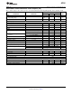


Table Of Contents
- FEATURES
- APPLICATIONS
- DESCRIPTION
- ABSOLUTE MAXIMUM RATINGS
- ELECTRICAL CHARACTERISTICS: Transmitter (Tx)
- ELECTRICAL CHARACTERISTICS: Power Amplifier (PA)
- ELECTRICAL CHARACTERISTICS: Receiver (Rx)
- ELECTRICAL CHARACTERISTICS: Digital
- ELECTRICAL CHARACTERISTICS: Two-Wire Interface
- ELECTRICAL CHARACTERISTICS: Internal Bias Generator
- ELECTRICAL CHARACTERISTICS: Power Supply
- THERMAL INFORMATION
- SPI TIMING REQUIREMENTS
- DEVICE INFORMATION
- TYPICAL CHARACTERISTICS
- APPLICATION INFORMATION
- Revision History

AFE031
SBOS531D –AUGUST 2010–REVISED MAY 2012
www.ti.com
ELECTRICAL CHARACTERISTICS: Receiver (Rx)
At T
J
= +25°C, PA_V
S
= 16 V, V
AVDD
= V
DVDD
= 3.3 V, and 10 kΩ connected to PA_ISET (pin 46), unless otherwise noted.
AFE031
PARAMETER CONDITIONS MIN TYP MAX UNIT
Rx PGA1
Input
Input voltage range 10 V
PP
G = 2 V/V 10 kΩ
G = 1 V/V 15 kΩ
Input resistance R
I
G = 0.5 V/V 20 kΩ
G = 0.25 V/V 24 kΩ
Frequency Response
G = 2 V/V 6 MHz
G = 1 V/V 10 MHz
Bandwidth BW
G = 0.5 V/V 13 MHz
G = 0.25 V/V 15 MHz
Output
Voltage output swing from
V
O
R
LOAD
= 6 kΩ, connected to AV
DD
/2 10 100 mV
AGND or AV
DD
Sourcing 25 mA
Maximum continuous current, dc I
O
Sinking 25 mA
Output resistance R
O
G = 1, f = 100 kHz 1 Ω
Gain
G = 0.25 V/V –1 ±0.1 +1 %
G = 0.5 V/V –1 ±0.1 +1 %
Gain error
G = 1 V/V –1 ±0.1 +1 %
G = 2 V/V –2 ±0.2 +2 %
Gain error drift T
J
= –40°C to +125°C 1 ppm/°C
Rx Filter
Input
Input voltage range GND – 0.1 AV
DD
+ 0.1 V
Input resistance R
IN
6 kΩ
Frequency Response
CENELEC A Mode Rx_C1 = 680 pF, Rx_C2 = 680 pF
Passband frequency –3 dB 90 kHz
Stop band attentuation –25 –33 dB
Stop band frequency 270 kHz
Filter gain 0 dB
CENELEC B/C/D Modes Rx_C1 = 270 pF, Rx_C2 = 560 pF
Passband frequency –3 dB 145 kHz
Stop band attentuation –23 –27 dB
Stop band frequency 350 kHz
Filter gain 0 dB
Output
Voltage output swing from
V
O
R
LOAD
= 10 kΩ, connected to AV
DD
/2 10 100 mV
AGND or AV
DD
Sourcing 25 mA
Maximum continuous current, dc I
O
Sinking 25 mA
Output resistance R
O
f = 100 kHz 5 Ω
6 Copyright © 2010–2012, Texas Instruments Incorporated
Product Folder Link(s): AFE031