
Datasheet


www.ti.com
THEORY OF OPERATION
The ADS8382 is a high-speed successive approximation register (SAR) analog-to-digital converter (ADC). The
REFERENCE
ADS8382
REFM
REFIN
REFOUT
AGND
0.1 F
1 F
ADS8382
REFM
REFIN
REFOUT
AGND
0.1 F
1 F
REF3040
22 F
50
AGND
ADS8382
SLAS416B – JUNE 2004 – REVISED NOVEMBER 2004
architecture is based on charge redistribution, which inherently includes a sample/hold function.
The device includes a built-in conversion clock, internal reference, and 40-MHz SPI compatible serial interface.
The maximum conversion time is 1.1 µ s which is capable of sustaining a 600-kHz throughput.
The analog input is provided to the two input pins: +IN and –IN. When a conversion is initiated, the differential
input on these pins is sampled on the internal capacitor array. While a conversion is in progress, both inputs are
disconnected from any internal function.
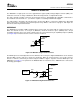
The ADS8382 has a built-in 4.096-V (nominal value) reference but can operate with an external reference also.
When the internal reference is used, pin 9 (REFOUT) should be shorted to pin 8 (REFIN) and a 0.1-µF
decoupling capacitor and a 1-µF storage capacitor must be connected between pin 8 (REFIN) and pin 7 (REFM)
(see Figure 50 ). The internal reference of the converter is buffered.
Figure 50. ADS8382 Using Internal Reference
The REFIN pin is also internally buffered. This eliminates the need to put a high bandwidth buffer on the board to
drive the ADC reference and saves system area and power. When an external reference is used, the reference
must be of low noise, which may be achieved by the addition of bypass capacitors from the REFIN pin to the
REFM pin. See Figure 51 for operation of the ADS8382 with an external reference. REFM must be connected to
the analog ground plane.
Figure 51. ADS8382 Using External Reference
21