
Datasheet


1
20
CLOCK
CONVST
andRD
M1
CONVST
andRD
SDOx
(1)
BUSY
16-bitdata 2n -
CHxx
1
1
20
C
H
x
conversion 1n -
ofbothCHxx
16-bitdatan
CH 0x
16-bitdatan+1
CH 1x
conversionn
ofbothCH 0x
16-bitdatan+2
CH 0x
conversionn+2
ofbothCH 0x
20
1
20
1
16-bitdata 1n -
CHxx
C
H
x
20
1
conversionn+3
ofbothCH 1x
conversionn+1
ofbothCH 1x
conversionn 1-
ofbothCHxx
16-bitdatan
CH 0x
16-bitdata 1n -
CHxx
C
H
x
conversionn
ofbothCH 0x
SDOx
(1)
BUSY
Full-ClockMode
Half-ClockMode
C
H
0
C
H
1
C
H
0
conversionn+1
ofbothCH 1x
C
H
1
M0
C
H
0
ADS8363
ADS7263
ADS7223
SBAS523B –OCTOBER 2010–REVISED JANUARY 2011
www.ti.com
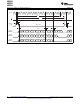
Mode III
This mode can be used for fully- or
pseudo-differential inputs (in pseudo-differential mode
With M0 = '1' and M1 = '0', the device automatically
the sequencer is used to control the input
cycles between the differential inputs (CONFIG
multiplexer). Channel information is available in
register bits C[1:0] are ignored) while offering the
fully-differential mode only if CID = '0' (CID is forced
conversion result of CHAx on SDOA and the
to '1' in pseudo-differential mode).
conversion result of CHBx on SDOB, as shown in
Figure 37.
The internal FIFO is available in this mode; when
used, a single read pulse allows for reading of all
Output data consist of a channel indicator ('0' for
stored conversion data. The FIFO should be
CHx0, or '1' for CHx1), followed by a '0', and then 16,
completely filled when used for the first time in order
14, or 12 bits of conversion result along with any
to ensure proper functionality.
trailing zeroes.
(1) ADS7263/7223 output data with the MSB located as ADS8363 and the last 2/4 bits being '0'.
Figure 37. Mode III Timing
(M0 = '1', M1 = '0', PDE = '0', CID = '0', Fully-Differential Example)
32 Submit Documentation Feedback Copyright © 2010–2011, Texas Instruments Incorporated
Product Folder Link(s): ADS8363 ADS7263 ADS7223