
Datasheet


conversionn
datan
CLOCK
CS
CONVST
BUSY
RD
SDOx
(1)
t
CLKL
t
1
SDI
RD
SDOx
(1)
SDI
(CID= ‘0’)
(CID= ‘1’)
t
CLK
t
2
t
D2
t
H1
t
S1
t
D5
t
H4
t
D4
datan
t
S2
t
H2
t
D6
t
D1
t
S2
t
H2
t
D5
t
H4
t
D4
t
CONV
t
ACQ
t
CLKH
1
23 4125 36
t
DATA
CH
0/1
M
S
B
D
14
D
13
D
12
D
11
D
10
D9 D8 D7 D6 D5 D4 D3 D0 D1 D0
D
15
D
14
D
13
D
12
D
11
D
10
D9 D8 D7 D6 D5 D4 D3 D2 D1 D0
M
S
B
D
14
D
13
D
12
D
11
D
10
D9 D8 D7 D6 D5 D4 D3 D2 D1 D0
D
15
D
14
D
13
D
12
D
11
D
10
D9 D8 D7 D6 D5 D4 D3 D2 D1 D0
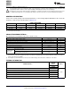
AD
A/B
ADS8363
ADS7263
ADS7223
SBAS523B –OCTOBER 2010–REVISED JANUARY 2011
www.ti.com
TIMING DIAGRAMS (continued)
(2) The ADS7263/7223 output data with the MSB located as ADS8363 and last 2/4 bits being '0'.
Figure 2. Detailed Timing Diagram: Full-Clock Mode
10 Submit Documentation Feedback Copyright © 2010–2011, Texas Instruments Incorporated
Product Folder Link(s): ADS8363 ADS7263 ADS7223