
Datasheet


DeviceinHoldMode;LastInputSampledfromIN
0
MUXOUT ADCIN
IN
0
IN
X
COM
50W
50W
AGND
VA
4pF
ESD
ESD
ESD
ESD
ESD
AGND
40W
55W
40pF
40pF
ESD
ADS8331
ADS8332
SBAS363C –DECEMBER 2009–REVISED MAY 2012
www.ti.com
THEORY OF OPERATION
DESCRIPTION
The ADS8331/32 is a high-speed, low-power, successive approximation register (SAR) analog-to-digital
converter (ADC) that uses an external reference. The architecture is based on charge redistribution, which
inherently includes a sample/hold function.
The ADS8331/32 has an internal clock that is used to run the conversion. However, the ADS8331/32 can be
programmed to run the conversion based on the external serial clock (SCLK).
The analog input to the ADS8331/32 is provided to two input pins: one of the IN
X
input channels and the shared
COM pin. When a conversion is initiated, the differential input on these pins is sampled on the internal capacitor
array. While a conversion is in progress, both IN
X
and COM inputs are disconnected from any internal function.
The ADS8331 has four analog inputs while the ADS8332 has eight inputs. All inputs share the same common
pin, COM. Both the ADS8331 and ADS8332 can be programmed to select a channel manually or can be
programmed into the auto channel select mode to sweep through the input channels automatically.
SIGNAL CONDITIONING
The ADS8331/32 has the flexibility to add signal conditioning between the MUXOUT and ADCIN pins, such as a
programmable gain amplifier (PGA) or filter. This feature reduces the system component count and cost because
each input channel does not require separate signal conditioning circuits, especially if the source impedance
connected to each channel is similar in value.
ANALOG INPUT
When the converter enters the hold mode, the voltage difference between the IN
X
and COM inputs is captured
on the internal capacitor array. The voltage on the COM pin is limited between (AGND – 0.2V) and (AGND +
0.2V). This limitation allows the ADS8331/32 to reject small signals that are common to both the IN
X
and COM
inputs. The IN
X
inputs have a range of –0.2V to (VA + 0.2V). The input span of (IN
X
– COM) is limited to 0V to
V
REF
.
The peak input current through the analog inputs depends upon a number of factors: reference voltage, sample
rate, input voltage, and source impedance. The current flowing into the ADS8331/32 charges the internal
capacitor array during the sample period. After this capacitance has been fully charged, there is no further input
current. The source of the analog input voltage must be able to charge the maximum input capacitance (45pF) to
a 16-bit settling level within the minimum acquisition time (238ns). When the converter goes into hold mode, the
input impedance is greater than 1GΩ.
Care must be taken regarding the absolute analog input voltage. To maintain linearity of the converter, the IN
X
inputs, the COM input, and the input span of (IN
X
– COM) should be within the limits specified. If these inputs are
outside of these ranges, the linearity of the converter may not meet specifications. To minimize noise, low-
bandwidth input signals with low-pass filters should be used. Care should be taken to ensure that the output
impedance of the sources driving the IN
X
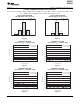
and COM inputs are matched, as shown in Figure 34. If this matching
is not observed, the two inputs could have different settling times, which may result in an offset error, gain error,
and linearity error that change with temperature and input voltage.
Figure 34. Input Equivalent Circuit
18 Copyright © 2009–2012, Texas Instruments Incorporated