
Datasheet


ADS8329
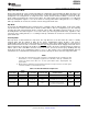
+IN
-IN
THS4031
20 W
20 W
470pF
50 W
Input
Signal
(0Vto4V)
5V
+VA
ADS8329
+IN
-IN
THS4031
20 W
20 W
1VDC
Input
Signal
(-2Vto2V)
5V
+VA
470pF
600 W
600 W
REFERENCE
CONVERTER OPERATION
ADS8329
ADS8330
SLAS516C – DECEMBER 2006 – REVISED JULY 2009 ...................................................................................................................................................
www.ti.com
Figure 52. Unipolar Input Drive Configuration
Figure 53. Bipolar Input Drive Configuration
The ADS8329/30 can operate with an external reference with a range from 0.3 V to 5 V. A clean, low noise,
well-decoupled reference voltage on this pin is required to ensure good performance of the converter. A low
noise band-gap reference like the REF3240 can be used to drive this pin. A 22- µ F ceramic decoupling capacitor
is required between the REF+ and REF – pins of the converter. These capacitors should be placed as close as
possible to the pins of the device. The REF – should be connected to its own via to the analog ground plane with
the shortest possible distance.
The ADS8329/30 has an oscillator that is used as an internal clock which controls the conversion rate. The
frequency of this clock is 21 MHz minimum. The oscillator is always on unless the device is in the deep
power-down state or the device is programmed for using SCLK as the conversion clock (CCLK). The minimum
acquisition (sampling) time takes 3 CCLKs (this is equivalent to 120 ns at 24.5 MHz) and the conversion time
takes 18 conversion clocks (CCLK) ( ≈ 780 ns) to complete one conversion.
The conversion can also be programmed to run based on the external serial clock, SCLK, if is so desired. This
allows a system designer to achieve system synchronization. The serial clock SCLK, is first reduced to 1/2 of its
frequency before it is used as the conversion clock (CCLK). For example, with a 42-MHz SCLK this provides a
21-MHz clock for conversions. If it is desired to start a conversion at a specific rising edge of the SCLK when the
external SCLK is programmed as the source of the conversion clock (CCLK) (and manual start of conversion is
selected), the setup time between CONVST and that rising SCLK edge should be observed. This ensures the
conversion is complete in 18 CCLKs (or 36 SCLKs). The minimum setup time is 20 ns to ensure synchronization
between CONVST and SCLK. In many cases the conversion can start one SCLK period (or CCLK) later which
results in a 19 CCLK (or 37 SCLK) conversion. The 20 ns setup time is not required once synchronization is
relaxed.
24 Submit Documentation Feedback Copyright © 2006 – 2009, Texas Instruments Incorporated
Product Folder Link(s): ADS8329 ADS8330