
Datasheet


DB6
DB5
DB4
DB3
DB2
DB1
DB0
NC
NC
+V
A
AGND
+IN
-IN
REF
OUT
REF
IN
-
DB15
DB14
DB13
DB12
DB11
DB10
DB9
DB8
1
2
3
4
5
6
7
8
24
23
22
21
20
19
18
17
CS
BYTE
RD
CONVST
CLOCK
DGND
+V
D
BUSY
DB7
ChipSelect
ReadInput
ConversionStart
ClockInput
BusyOutput
+
AnalogInput
9 10
11 12
13
14
15 16
32 31 30 29 28
ADS8322
27 26 25
0.1mF
10mF
+5VAnalogSupply
+
0.1mF
ADS8322
www.ti.com
SBAS215A –JULY 2001–REVISED JANUARY 2010
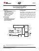
THEORY OF OPERATION
The ADS8322 is a high-speed successive times are at least 40ns and the clock period is at
approximation register (SAR) A/D converter with an least 100ns. The minimum clock frequency is
internal 2.5V bandgap reference. The architecture is governed by the parasitic leakage of the capacitive
based on capacitive redistribution, which inherently digital-to-analog (CDAC) capacitors internal to the
includes a sample-and-hold function. The basic ADS8322.
operating circuit for the ADS8322 is shown in
The analog input is provided to two input pins, +IN
Figure 13.
and –IN. When a conversion is initiated, the
The ADS8322 requires an external clock to run the differential input on these pins is sampled on the
conversion process. The clock can be run internal capacitor array. While a conversion is in
continuously or it can be gated to conserve power progress, both inputs are disconnected from any
between conversions. This clock can vary between internal function.
25kHz (1.25kHz throughput) and 10MHz (500kHz
throughput). The duty cycle of the clock is
unimportant as long as the minimum HIGH and LOW
Figure 13. Typical Circuit Configuration
Copyright © 2001–2010, Texas Instruments Incorporated Submit Documentation Feedback 9
Product Folder Link(s): ADS8322