
Datasheet


ADS8320
9
SBAS108D
www.ti.com
NOISE
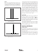
The noise floor of the ADS8320 itself is extremely low, as
can be seen from Figures 1 and 2, and is much lower than
competing A/D converters. It was tested by applying a low-
noise DC input and a 5.0V reference to the ADS8320 and
initiating 5000 conversions. The digital output of the A/D
2
2510
3
2490
4
Code
56
0000
1
FIGURE 1. Histogram of 5000 Conversions of a DC Input
at the Code Transition.
FIGURE 2. Histogram of 5000 Conversions of a DC Input
at the Code Center.
2
72
3
4864
4
Code
56
64 000
1
converter varies in output code due to the internal noise of
the ADS8320. This is true for all 16-bit SAR-type A/D
converters. Using a histogram to plot the output codes, the
distribution should appear bell-shaped with the peak of the
bell curve representing the nominal code for the input value.
The ±1σ, ±2σ, and ±3σ distributions represents the 68.3%,
95.5%, and 99.7%, respectively, of all codes. The transition
noise can be calculated by dividing the number of codes
measured by 6 and this yields the ±3σ distribution or 99.7%
of all codes. Statistically, up to 3 codes could fall outside the
distribution when executing 1000 conversions. The
ADS8320, with < 3 output codes for the ±3σ distribution,
yields a < ±0.5LSB transition noise. Remember, to achieve
this low noise performance, the peak-to-peak noise of the
input signal and reference must be < 50µV.
AVERAGING
The noise of the A/D converter can be compensated by
averaging the digital codes. By averaging conversion re-
sults, transition noise is reduced by a factor of 1/√n, where
n is the number of averages. For example, averaging four
conversion results reduces the transition noise by 1/2 to
±0.25 LSBs. Averaging should only be used for input
signals with frequencies near DC.
For AC signals, a digital filter can be used to low-pass filter
and decimate the output codes. This works in a similar
manner to averaging; for every decimation by 2, the signal-
to-noise ratio improves 3dB.
DIGITAL INTERFACE
SIGNAL LEVELS
The digital inputs of the ADS8320 can accommodate logic
levels up to 5.5V regardless of the value of V
CC
. Thus, the
ADS8320 can be powered at 3V and still accept inputs from
logic powered at 5V.
The CMOS digital output (D
OUT
) swings 0V to V
CC
. If V
CC
is 3V and this output is connected to a 5V CMOS logic
input, then that IC may require more supply current than
normal and may have a slightly longer propagation delay.