
Datasheet


OPA365
47 F,
1.5 ESR
(HighESR)
m
W
10 Fm
50 W
REF5050
+
-
4.7 F,
LowESR
m
+
-
ADS8318
IN+
IN-
REFIN
OUT
TRIM
-
+
47 F,
1.5 ESR
(HighESR)
m
W
22 Fm
REF5050
+
-
+
-
ADS8318
IN+
IN-
REFIN
OUT
TRIM
4.7 F,
LowESR
m
ADS8318
SLAS568A –MAY 2008– REVISED MARCH 2011
www.ti.com
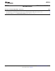
Figure 60. External Reference Driving Circuit
Figure 61. Direct External Reference Driving Circuit
POWER SAVING
The ADS8318 has an auto power-down feature. The device powers down at the end of every conversion. The
input signal is acquired on sampling capacitors while the device is in the power-down state, and at the same time
the conversion results are available for reading. The device powers up by itself on the start of the conversion. As
discussed before, the conversion runs on an internal clock and takes a fixed time. As a result, device power
consumption is directly proportional to the speed of operation.
DIGITAL OUTPUT
As discussed before (in the DESCRIPTION and TIMING DIAGRAMS sections) the device digital output is SPI
compatible. The following table lists the output codes corresponding to various analog input voltages.
DESCRIPTION ANALOG VALUE (V) DIGITAL OUTPUT STRAIGHT BINARY
Full-scale range 2*V
ref
Least significant bit (LSB) 2*V
ref
/65536 BINARY CODE HEX CODE
Positive full scale +V
ref
– 1 LSB 0111 1111 1111 1111 7FFF
Midscale 0 V 0000 0000 0000 0000 0000
Midscale – 1 LSB 0 – 1 LSB 1111 1111 1111 1111 FFFF
Negative full scale –V
ref
1000 0000 0000 0000 8000
SCLK INPUT
The device uses SCLK for serial data output. Data is read after the conversion is over and the device is in the
acquisition phase. It is possible to use a free running SCLK for the device, but it is recommended to stop the
clock during a conversion, as the clock edges can couple with the internal analog circuit and can affect
conversion results.
22 Submit Documentation Feedback Copyright © 2008–2011, Texas Instruments Incorporated
Product Folder Link(s): ADS8318