
Datasheet


1 2
15
16
CONVST
ACQUISITION
CONVERSION ACQUISITION
SCLK
SDO
t
1
t
en
t
dis
t
2
t
3
t
clkh
t
clkl
t
clk
D15
D14 D1
D0
t
cnv
t
acq
t
cyc
CONVST
SCLK
SDO
CNV
CLK
SDI
SDI
ADS8318
DigitalHost
IRQ
+
VBD
ADS8318
SLAS568A –MAY 2008– REVISED MARCH 2011
www.ti.com
When the conversion is over, the device enters the acquisition phase and powers down. On the falling edge of
CONVST, SDO comes out of three state, and the device outputs the MSB of the data. After this, the device
outputs the next lower data bits on every falling edge of SCLK. SDO goes to 3-state after the 16
th
falling edge of
SCLK or CONVST high, whichever occurs first. It is necessary that the device sees a minimum of 15 falling
edges of SCLK during the low period of CONVST.
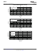
Figure 46. Interface Timing Diagram, 3 Wire CS Mode Without Busy Indicator (SDI = 1)
3 Wire CS Mode With Busy Indicator
Figure 47. Connection Diagram, 3 Wire CS Mode With Busy Indicator
The three wire interface option in CS mode is selected if SDI is tied to +VBD (see Figure 47). In the three wire
interface option, CONVST acts like CS. As shown in Figure 48, the device samples the input signal and enters
the conversion phase on the rising edge of CONVST, at the same time SDO goes to 3 state. Conversion is done
with the internal clock and it continues irrespective of the state of CONVST. As a result it is possible to toggle
CONVST (acting as CS) after the start of the conversion to select other devices on the board. But it is absolutely
necessary that CONVST is low again before the minimum conversion time (t
cnv
in timing requirements table) is
elapsed and continues to stay low until the end of maximum conversion time. A low level on the CONVST input
at the end of a conversion ensures the device generates a busy indicator.
When the conversion is over, the device enters the acquisition phase and powers down, and the device forces
SDO out of three state and outputs a busy indicator bit (low level). The device outputs the MSB of data on the
first falling edge of SCLK after the conversion is over and continues to output the next lower data bits on every
subsequent falling edge of SCLK. SDO goes to three state after the 17
th
falling edge of SCLK or CONVST high,
whichever occurs first. It is necessary that the device sees a minimum of 16 falling edges of SCLK during the low
period of CONVST.
14 Submit Documentation Feedback Copyright © 2008–2011, Texas Instruments Incorporated
Product Folder Link(s): ADS8318