
Datasheet


www.ti.com
ADS820
11
SBAS037B
AC performance. It is important to select a transformer that
gives low distortion and does not exhibit core saturation at
full-scale voltage levels. Since the transformer does not
appreciably load the ladder, there is no need to buffer the CM
output in this instance. In general, it is advisable to keep the
current draw from the CM output pin below 0.5µA to avoid
nonlinearity in the internal reference ladder. A FET input
operational amplifier, such as the OPA130, can provide a
buffered reference for driving external circuitry. The analog
IN and
IN
inputs should be bypassed with 22pF capacitors to
minimize track-and-hold glitches and to improve high-input
frequency performance.
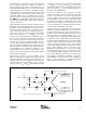
Figure 5 illustrates another possible low-cost interface circuit
that utilizes resistors and capacitors in place of a transformer.
Depending on the signal bandwidth, the component values
should be carefully selected in order to maintain the perfor-
mance outlined in the data sheet. The input capacitors, C
IN
,
and the input resistors, R
IN
, create a high-pass filter with the
lower corner frequency at f
C
= 1/(2πR
IN
C
IN
). The corner
frequency can be reduced by either increasing the value of
R
IN
or C
IN
. If the circuit operates with a 50Ω or 75Ω imped-
ance level, the resistors are fixed and only the value of the
capacitor can be increased. Usually AC-coupling capacitors
are electrolytic or tantalum capacitors with values of 1µF or
higher. It should be noted that these large capacitors become
inductive with increased input frequency, which could lead to
signal amplitude errors or oscillation. To maintain a low ac-
coupling impedance throughout the signal band, a small
value (e.g. 1µF) ceramic capacitor could be added in parallel
with the polarized capacitor.
Capacitors C
SH1
and C
SH2
are used to minimize current
glitches resulting from the switching in the input track and
hold stage and to improve signal-to-noise performance. These
capacitors can also be used to establish a low-pass filter and
effectively reduce the noise bandwidth. In order to create a
real pole, resistors R
SER1
and R
SER2
were added in series with
each input. The cutoff frequency of the filter is determined by
f
C
= 1/(2πR
SER
• (C
SH
+ C
ADC
)) where R
SER
is the resistor in
series with the input, C
SH
is the external capacitor from the
input to ground, and C
ADC
is the internal input capacitance of
the A/D converter (typically 4pF).
Resistors R
1
and R
2
are used to derive the necessary
common-mode voltage from the buffered top and bottom
references. The total load of the resistor string should be
selected so that the current does not exceed 1mA. Although
the circuit in Figure 5 uses two resistors of equal value so that
the common-mode voltage is centered between the top and
bottom reference (+2.25V), it is not necessary to do so. In all
cases the center point, V
CM
, should be bypassed to ground in
order to provide a low-impedance ac ground.
If the signal needs to be DC-coupled to the input of the
ADS820, an operational amplifier input circuit is required. In
the differential input mode, any single-ended signal must be
modified to create a differential signal. This can be accom-
plished by using two operational amplifiers; one in the
noninverting mode for the input and the other amplifier in the
inverting mode for the complementary input. The low distor-
tion circuit in Figure 6 will provide the necessary input shifting
required for signals centered around ground. It also employs
a diode for output level shifting to ensrue a low distortion
+3.25V output swing. Another DC-coupled circuit is shown in
Figure 7. Other amplifiers can be used in place of the
OPA860s if the lowest distortion is not necessary. If output
level shifting circuits are not used, care must be taken to
select operational amplifiers that give the necessary perfor-
mance when swinging to +3.25V with a ±5V supply opera-
tional amplifier. The OPA620 and OPA621, or the lower
power OPA820 can be used in place of the OPA860s in
Figure 6. In that configuration, the OPA820 will typically
swing to within 100mV of positive full scale.
FIGURE 5. AC-Coupled Differential Input Circuit.
ADS8xx
R
SER1
(1)
49.9Ω
R
3
1kΩ
R
2
(6kΩ)
R
1
(6kΩ)
C
2
0.1µF
C
SH1
22pF
C
SH2
22pF
C
3
0.1µF
C
1
0.1µF
C
IN
0.1µF
V
CM
C
IN
0.1µF
R
IN1
25Ω
R
IN2
25Ω
R
SER2
(1)
49.9Ω
+3.25V
Top Reference
+1.25V
Bottom Reference
IN
NOTE: (1) indicates optional component.
IN