
Datasheet


ADS807
10
SBAS072A
www.ti.com
will improve the SNR performance, but depending on the
signal source, large resistor values may be detrimental to
achieving good harmonic distortion. In any case, optimizing
the R-C values for the specific application is encouraged.
Transformer Coupled, Single-Ended to Differential
Configuration
If the application requires a signal conversion from a single-
ended source to drive the ADS807 differentially, an RF
transformer might be a good solution. The selected trans-
former must have a center tap in order to apply the common-
mode DC voltage necessary to bias the converter inputs. AC-
grounding the center tap will generate the differential signal
swing across the secondary winding. Consider a step-up
transformer to take advantage of a signal amplification with-
out the introduction of another noise source. Furthermore,
the reduced signal swing from the source may lead to
improved distortion performance.
The differential input configuration provides a noticeable
advantage of achieving good SFDR over a wide range of
input frequencies. In this mode, both inputs of the ADS807
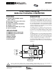
see matched impedances. Figure 1 shows the schematic for
the suggested transformer coupled interface circuit. The
component values of the R-C low-pass may be optimized
depending on the desired roll-off frequency. The resistor
across the secondary side (R
T
) should be calculated using
the equation R
T
= n
2
• R
G
to match the source impedance
(R
G
) for good power transfer and VSWR.
The circuit example of Figure 1 shows the voltage-feedback
amplifier OPA680 driving the RF transformer, which converts
the single-ended signal into a differential one. The OPA680
can be employed for either single- or dual-supply operation.
For details on how to optimize its frequency response, refer
to the OPA680 data sheet (SBOS083), available at
www.ti.com. With the 49.9Ω series output resistor, the ampli-
fier emulates a 50Ω source (R
G
). Any DC content of the
signal can be easily blocked by a capacitor (0.1µF) and to
also to avoid DC loading of the op amp’s output stage.
AC-Coupled, Single-Ended-to-Differential Interface
with Dual-Supply Op Amps
Communications applications, in particular, demand a very
high dynamic range and low levels of intermodulation distor-
tion, but usually allow the input signal to be AC-coupled into
the A/D converter. Appropriate driver amplifiers need to be
selected to maintain the excellent distortion performance of
the ADS807. Often, these op amps deliver the lowest distor-
tion with a small, ground-centered signal swing that requires
dual power supplies. Because of the AC-coupling, this re-
quirement can be easily accomplished and the needed level
shifting of the input signal can be implemented without
affecting the driver circuit.
See Figure 2 for an example of such an interface circuit
specifically designed to maximize the dynamic performance.
The voltage feedback amplifier, OPA642, maintains an ex-
cellent distortion performance for input frequencies of up to
15MHz. The two amplifiers (A1, A2) are configured as an
inverting and noninverting gain stage to convert the input
signal from single-ended to differential. The nominal gain for
this stage is set to +2V/V. The outputs of the OPA642s are
AC-coupled to the converter’s differential inputs. This will
keep the distortion performance at its best since the signal
range stays within the linear region of the op amp and
sufficient headroom to the supply rails can be maintained.
Four resistors located between the top (REFT) and bottom
(REFB) reference shift the input signal to a common-mode
voltage of approximately +2.5V.
The interface circuit of Figure 2 can be modified to extend
the bandwidth to approximately 25MHz by replacing the
OPA642 with its decompensated version, the OPA643. The
OPA643 provides the necessary slew rate for a low distortion
front end to the ADS807. With a minimum gain stability of +3,
the gain resistors have to be modified, as well as optimizing
the series resistor and shunt capacitance at each of the
converter inputs.
FIGURE 1. Converting a Single-Ended Input Signal into a Differential Signal Using a RF-Transformer.
V
IN
IN
IN
CM
+2.5V
24.9Ω
24.9Ω
47pF
R
T
47pF
10µF
0.1µF
1:n
0.1µF
R
G
R
2
R
1
OPA680
49.9Ω
ADS807E
+