
Datasheet


Deviceinanyoperationmode
Yes
No
CS
CS
Auto 2 register
programming
Program Auto2register?
SDI:Di15..12=1001
DI9..6=binaryaddressoflastchannelinthesequence
refertables6
Endof Auto2registerprogramming
ADS7950, ADS7951, ADS7952, ADS7953
ADS7954, ADS7955, ADS7956, ADS7957
ADS7958, ADS7959, ADS7960, ADS7961
SLAS605A –JUNE 2008–REVISED JANUARY 2010
www.ti.com
Table 5. Mode Control Register Settings for Auto-2 Mode
DESCRIPTION
RESET
BITS
LOGIC
STATE
FUNCTION
STATE
DI15-12 0001 0011 Selects Auto-2 Mode
DI11 0 1 Enables programming of bits DI10-00.
0 Device retains values of DI10-00 from the previous frame.
DI10 0 1 Channel number is reset to Ch-00.
0 Channel counter increments every conversion.(No reset).
DI09-07 000 xxx Do not care
DI06 0 0 Selects 2.5V i/p range (Range 1)
1 Selects 5V i/p range (Range 2)
DI05 0 0 Device normal operation (no powerdown)
1 Device powers down on the 16th SCLK falling edge
DI04 0 SDO outputs the current channel address of the channel on DO15..12 followed by the 12-bit
0
conversion result on DO11..00.
1 GPIO3-GPIO0 data (both input and output) is mapped onto DO15-DO12 in the order shown below.
Lower data bits DO11-DO00 represent the 12-bit conversion result of the current channel.
DO15 DO14 DO13 DO12
GPIO3
(1)
GPIO2
(1)
GPIO1
(1)
GPIO0
(1)
DI03-00 0000 GPIO data for the channels configured as output. Device ignores data for the channel which is configured as
input. SDI bit and corresponding GPIO information is given below
DI03 DI02 DI01 DI00
GPIO3
(1)
GPIO2
(1)
GPIO1
(1)
GPIO0
(1)
(1) GPIO 1 to 3 are available only in TSSOP packaged devices. QFN device offers GPIO 0 only.
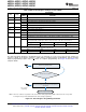
The Auto-2 Program Register is programmed (once on powerup or reset) to pre-select the last channel (or
sequence depth) in the Auto-2 sequence. Unlike Auto-1 Program Register programming, Auto-2 Program
Register programming requires only 1 CS frame for complete programming. See Figure 54 and Table 6 for
complete details.
NOTE: The device continues its operation in the selected mode during programming. SDO is valid, however it is not possible
to change the range or write GPIO data into the device during programming.
Figure 54. Auto-2 Register Programming Flowchart
34 Submit Documentation Feedback Copyright © 2008–2010, Texas Instruments Incorporated
Product Folder Link(s): ADS7950, ADS7951, ADS7952, ADS7953 ADS7954, ADS7955, ADS7956, ADS7957 ADS7958,
ADS7959, ADS7960, ADS7961