
Datasheet


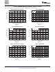


Table Of Contents
- FEATURES
- APPLICATIONS
- DESCRIPTION
- ABSOLUTE MAXIMUM RATINGS
- THERMAL INFORMATION
- ELECTRICAL CHARACTERISTICS: ADS7947 (12-Bit)
- ELECTRICAL CHARACTERISTICS: ADS7948 (10-Bit)
- ELECTRICAL CHARACTERISTICS: ADS7949 (8-Bit)
- TIMING DIAGRAM
- TIMING REQUIREMENTS
- PIN CONFIGURATION
- TYPICAL CHARACTERISTICS: ADS7947, ADS7948, ADS7949
- TYPICAL CHARACTERISTICS: ADS7947 (12-Bit)
- OVERVIEW
- DEVICE OPERATION
- APPLICATION INFORMATION

12W
AIN0P
AIN1P
AIN0N
AIN1N
32pF
32pF
12W
12W
12W
1 2 3 N
(1)
SCLK
CS
Sample
N(AIN0)
Sample
N+1(AIN1)
t
ACQ
AcquisitionofAIN1
t
CONV
ConversionofSampleN
1 2
Sample
N+2(AIN0)
Windowfor
CHSELToggle
DoNotToggleCHSEL
inThisWindow
CHSEL
t
CONV
ConversionofSampleN+1
t
ACQ
AcquisitionofAIN0
3 N
(1)
ADS7947
ADS7948
ADS7949
www.ti.com
SLAS708 –SEPTEMBER 2010
Figure 39 shows an equivalent circuit of the multiplexer and ADC sampling stage. The positive and negative
inputs are separately sampled on 32pF sampling capacitorss. The multiplexer and sampling switches are
represented by an ideal switch in series with a 12Ω resistance. During sampling, the devices connect the 32pF
sampling capacitor to the ADC driver. This connection creates a glitch at the device input. It is recommended to
connect a capacitor across the AINxP and AINxN terminals to reduce this glitch. A driving circuit must have
sufficient bandwidth to settle this glitch within the acquisition time.
Figure 39. Input Sampling Stage Equivalent Circuit
(See the Application Information section for details on the driving circuit.)
Figure 40 shows a timing diagram for the ADC analog input channel selection. As shown in Figure 40, the CH
SEL signal selects the analog input channel to the ADC. CH SEL = 0 selects channel 0 ( AIN0P – AIN0N) and
CH SEL = 1 selects channel 1 ( AIN1P – AIN1N). It is recommended not to toggle the CH SEL signal during an
ADC acquisition phase until the device sees the first valid SCLK rising edge after the device samples the analog
input. If CH SEL is toggled during this period, it can cause erroneous output code as the device might see
unsettled analog input.
CH SEL can be toggled at any time during the window specified in Figure 40; however, it is recommended to
select the desired channel after the first SCLK rising edge and before the second SCLK rising edge. This timing
ensures that the multiplexer output is settled before the ADC starts acquisition of the analog input.
(1) N indicates the 14th SCLK rising edge for the ADS7947 (12-bit) , the 11th rising edge for the ADS7948 (10-bit), and the ninth rising edge
for the ADS7949 (8-bit).
Figure 40. ADC Analog Input Channel Selection
Copyright © 2010, Texas Instruments Incorporated Submit Documentation Feedback 19
Product Folder Link(s): ADS7947 ADS7948 ADS7949