
Datasheet


12 W
AIN0P
AIN1P
AIN N0
AIN1N
32pF
32pF
12 W
12 W
12 W
ADS7945
12 W
AIN0
AIN1
AIN GND0
AIN1GND
32pF
32pF
12 W
12 W
12 W
ADS7946
1 2
3 16
SCLK
CS
t
SU1
SampleN
(AIN0)
SampleN+1
(AIN1)
t
ACQ
AcquisitionofAIN1
t
CONV
ConversionofSampleN
1 2
3 16
SampleN+2
(AIN0)
Windowfor
CHSELToggle
DoNotToggle
CHSELin
ThisWindow
CHSEL
t
CONV
ConversionofSampleN+1
t
ACQ
AcquisitionofAIN0
ADS7945
ADS7946
www.ti.com
SBAS539B –JUNE 2011– REVISED SEPTEMBER 2011
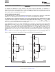
Figure 76 shows an equivalent circuit of the multiplexer and ADC sampling stage. See the Application
Information section for details on the driving circuit. The positive and negative/ground sense inputs are
separately sampled on 32 pF sampling capacitors. The multiplexer and sampling switches are represented by an
ideal switch in series with a 12 Ω resistance. Note that this is dc resistance and can be used for step-settling
calculations (do not use the RC values shown in Figure 76 for 3 dB bandwidth calculations for undersampling
applications). During sampling, the devices connect the 32 pF sampling capacitor to the ADC driver. This
connection creates a glitch at the device input. It is recommended to connect a capacitor across the AINxP and
AINxN terminals or AINx and AINxGND terminals to reduce this glitch for the ADS7945 or ADS7946,
respectively. A driving circuit must have sufficient bandwidth to settle this glitch within the acquisition time.
Figure 76. Input Sampling Stage Equivalent Circuit
Figure 77 shows a timing diagram for the ADC analog input channel selection. As shown in Figure 77, the CH
SEL signal selects the analog input channel to the ADC. CH SEL = 0 selects channel 0 and CH SEL = 1 selects
channel 1. It is recommended not to toggle the CH SEL signal during an ADC acquisition phase until the device
sees the first valid SCLK rising edge after the device samples the analog input. If CH SEL is toggled during this
period, it can cause erroneous output code because the device might see unsettled analog input.
CH SEL can be toggled at any time during the window specified in Figure 77; however, it is recommended to
select the desired channel after the first SCLK rising edge and before the second SCLK rising edge. This timing
ensures that the multiplexer output is settled before the ADC starts acquisition of the analog input.
Figure 77. ADC Analog Input Channel Selection
Copyright © 2011, Texas Instruments Incorporated Submit Documentation Feedback 25
Product Folder Link(s): ADS7945 ADS7946